Photosensitive Polymers: Negative vs. Positive Photoresist
A process sheet from a Japanese materials supplier lists the resist as "ポジ型" (poji-gata) and the dry film as "ネガ型" (nega-gata). The terms mean positive tone and negative tone. To run either material well, you need to know what light actually does to the polymer.
The short answer: a photosensitive polymer changes its properties, most often its solubility in a developer, where light hits it. In a negative-tone material, the exposed area hardens and stays after development. In a positive-tone material, the exposed area becomes soluble and washes away.
This guide covers the three light-driven reactions, the classic chemistry behind negative and positive resists, and how chemically amplified photoresists made modern chip patterning possible. It then looks at printed circuit boards, printing plates, UV-curable inks and coatings, and 3D printing. It ends with where Japanese suppliers stand, the Japanese terms you will see on their documents, and a list of questions to send them.
Contents
- What Is a Photosensitive Polymer?
- How Light Cures or Dissolves the Polymer
- Negative vs. Positive Photoresist
- Photolithography: Patterning Semiconductor Circuits
- Beyond Chips: PCBs, Printing Plates, UV Inks, and 3D Printing
- Japanese Photoresist Suppliers and Where They Stand
- Japanese Terms You Will See on Resist Documents
- Questions to Ask Your Resist or Dry Film Supplier
- Limits of This Overview
- FAQ
- Sources
What Is a Photosensitive Polymer?
A photosensitive polymer is any polymer whose structure changes under light or other radiation, which in turn changes properties such as solubility. As an industrial material, it is often called a photosensitive resin, or 感光性樹脂 (kankosei jushi) in Japanese. This article uses "photosensitive polymer" and "photosensitive resin" interchangeably.
The light-driven reactions fall into three groups: photo-crosslinking, photopolymerization, and photodecomposition. In each case, exposed and unexposed areas end up with different solubility, and that difference is what creates a pattern.
All three reactions create a solubility difference between exposed and unexposed areas.
Based on the classification of photosensitive resins in Japanese encyclopedias (Kotobank). Some photodecomposition systems, such as azides, become less soluble because the fragments go on to crosslink.
A second way to classify these materials looks at where the photoactive part sits. In one type, the polymer itself carries light-sensitive groups. In the other, a small light-sensitive molecule (a photosensitizer or photoactive compound) is blended into a polymer that does not react to light.
The two classifications use different axes, so one material can be described both ways.
How Light Cures or Dissolves the Polymer
Two classic textbook materials show the two directions clearly. Polyvinyl cinnamate becomes insoluble when exposed, while diazonaphthoquinone (DNQ)–novolac resists become soluble.
Polyvinyl Cinnamate: Crosslinked by Light
Polyvinyl cinnamate is the best-known photo-crosslinking polymer. Under light, side groups on one chain bond to side groups on a neighboring chain and form a network. The networked areas no longer dissolve in solvent, so only the exposed areas remain after development, which makes it a negative-tone material.
It is made by esterifying the hydroxyl groups of polyvinyl alcohol (PVA) with cinnamoyl chloride, the acid chloride of cinnamic acid. Cinnamic acid has a carbon–carbon double bond (C=C) next to a benzene ring, and that double bond absorbs the light and reacts.
The two steps, synthesis and crosslinking, look like this.
As crosslinks build up, the chains can no longer move freely, so the film becomes harder and less soluble. Photo-crosslinking systems like this were adopted early because of their high sensitivity. The cinnamate ester of PVA, first developed by Eastman Kodak in the US, was used as a photoresist for photoengraving.
DNQ–Novolac: Made Soluble by Light
The classic positive resist blends a photoactive compound called diazonaphthoquinone (DNQ) into novolac, a type of phenolic resin. In unexposed areas, DNQ slows the resin's dissolution. Light decomposes the DNQ into a carboxylic acid, so only the exposed areas dissolve in an alkaline developer.
Negative vs. Positive Photoresist
Photoresists are classified by what happens to the exposed area. In a negative resist, crosslinking or polymerization makes the exposed area insoluble, so it stays. In a positive resist, the exposed area becomes soluble in the developer and is removed, so the same mask produces the reverse pattern.
With the same mask, a negative resist keeps the exposed area and a positive resist keeps the unexposed area.
Gray: mask (opaque). Dark blue: resist remaining after development. Light blue: substrate. Based on the definitions in the 2013 Japan Prize achievement description.
The table below sums up the differences.
| Item | Negative tone | Positive tone |
|---|---|---|
| Reaction under light | Crosslinking or polymerization makes molecules larger | Photoactive compound decomposes or protecting groups come off, raising solubility |
| What remains after development | Exposed areas | Unexposed areas |
| Typical materials | Polyvinyl cinnamate, azide-based resists, acrylic photopolymer systems | DNQ–novolac, chemically amplified resists |
| Example uses | Photoengraving, PCB dry film resists, printing plates | Semiconductor patterning (g-line, i-line, KrF, ArF, and others) |
Photolithography: Patterning Semiconductor Circuits
Semiconductor manufacturing is the most important use of photosensitive polymers. A silicon wafer carries layers such as insulating silicon dioxide (SiO2), and trenches and holes must be etched into those layers only where wiring and devices go.
To mark which areas to etch, the fab coats the whole wafer with photoresist and exposes it through a photomask that carries the circuit pattern. Development removes the unwanted resist, and the remaining resist shields the layer beneath it during etching. This sequence is called photolithography.
Figure 3 shows the five basic steps in cross-section.
Development shapes the resist. Etching then removes the SiO2 underneath. The two steps do different jobs.
Dark blue: resist. Light blue: SiO2 oxide layer. White: silicon. Gray: mask. With a positive resist, the mask opening is reversed. Real processes also include bake steps after coating and after exposure.
With a negative resist, the resist in the mask's shadow never hardens, so the developer washes it away and exposes the SiO2. Hydrofluoric acid then dissolves only the SiO2 that the resist does not cover, leaving a trench.
The wet-etch reaction is shown below.
Once its job is done, the resist is removed with chemicals or plasma. A wafer goes through this coat-to-strip cycle once for each patterned layer, building up the circuit layer by layer.
Exposure Wavelengths: From g-Line to EUV
The basic way to print smaller features is to use a shorter exposure wavelength. Light sources moved from the g-line and i-line of mercury lamps to KrF and ArF excimer lasers, and then to extreme ultraviolet (EUV). Each change of light source required new resists matched to that wavelength.
The table lists each source with the resists typically used.
| Light source | Wavelength | Typical resist |
|---|---|---|
| g-line (mercury lamp) | 436 nm | DNQ–novolac (positive) |
| i-line (mercury lamp) | 365 nm | DNQ–novolac (positive) |
| KrF (krypton fluoride) excimer laser | 248 nm | Chemically amplified (polyhydroxystyrene-based) |
| ArF (argon fluoride) excimer laser | 193 nm | Chemically amplified (resin redesigned to transmit 193 nm light) |
| EUV (tin plasma source) | 13.5 nm | Mostly chemically amplified; metal oxide and other types under development |
Resists must be redesigned for each wavelength because a resin that absorbs the light too strongly keeps it from reaching the bottom of the film. Novolac absorbs KrF deep-UV light strongly, so KrF resists use a different resin backbone. For ArF, research on raising transparency at 193 nm started early.
An EUV source fires a laser at molten tin droplets about 25 µm in diameter, turning them into a plasma that emits 13.5 nm light.
Chemically Amplified Resists: One Acid, Many Reactions
As exposure wavelengths became shorter, conventional resists lost much of their sensitivity. In the early 1980s, Grant Willson, Jean Fréchet, and Hiroshi Ito at IBM developed the answer, a chemically amplified resist that uses light-generated acid as a catalyst for a chain of reactions.
In a chemically amplified resist, a photoacid generator (PAG) absorbs light and releases acid. During the post-exposure bake, that acid strips protecting groups from the resin one after another. The first practical version used polyhydroxystyrene with its hydroxyl groups capped by tBOC (tert-butoxycarbonyl) groups.
The deprotection reaction runs as follows.
Because one acid molecule acts many times, a small dose of light can change the solubility of the whole exposed film. IBM used this resist to produce 1-megabit DRAM. It came into wide use from the 250 nm generation onward and became essential for KrF lithography.
The same concept still underpins ArF, EUV, and electron-beam lithography, and Willson and Fréchet received the Japan Prize in 2013. Photoacid generators also drive the cationic polymerization of UV-curable resins covered below. The same "make acid with light" chemistry serves both chipmaking and coatings.
Beyond Chips: PCBs, Printing Plates, UV Inks, and 3D Printing
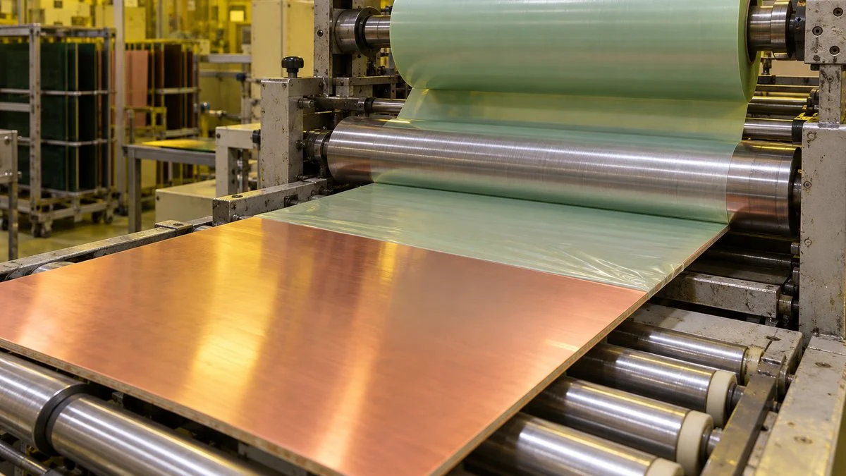
Outside semiconductor fabs, photosensitive polymers are used wherever it helps to change a material only where light hits it. The easiest way to compare the uses is to ask what light does and what finally happens to the exposed area.
The table compares five common uses.
| Use | What light does | Exposed area | What happens next |
|---|---|---|---|
| Semiconductor photoresist (chemically amplified) | Acid removes protecting groups | Dissolves in development (positive) | Remaining resist protects the layer during etching, then is removed |
| PCB dry film resist | Photopolymerization crosslinks the film | Stays (negative) | Copper is etched or plated to form traces, then the resist is removed |
| Photopolymer printing plate | Photopolymerization hardens the resin | Stays and forms the raised printing surface | Washed out with water and used as the plate |
| UV-curable coatings, adhesives, and inks | Polymerization or crosslinking hardens the resin | The whole layer hardens | No development; stays as part of the product |
| Vat photopolymerization 3D printing | Photopolymerization hardens the resin | Hardens one layer at a time | The hardened resin is the printed part |
PCB Dry Film Resist: Negative-Tone Photopolymerization
PCB fabrication uses dry film resist, a photosensitive layer sandwiched between films. It has three layers: a polyethylene cover film, the photosensitive layer, and a PET carrier film. The cover film is peeled off, and the resist is laminated to copper-clad laminate with heat and pressure before exposure.
The photosensitive layer is negative tone. A photoinitiator releases radicals under UV light, and these polymerize monomers into a network. In unexposed areas, the resin's carboxyl groups (−COOH) remain, and a sodium carbonate solution of about 1–2% neutralizes and dissolves them.
The development reaction is simple acid–base chemistry.
DuPont brought dry film into PCB production in the late 1960s under the Riston name. In Japan, Asahi Kasei's SUNFORT dry film is used in boards for PCs, smartphones, and automotive electronics.
In May 2025, Asahi Kasei announced a SUNFORT grade for redistribution layers in advanced semiconductor packages, such as those for AI servers. With laser direct imaging (LDI), it can form resist lines 1.0 µm wide.
Printing Plates: Water-Washable Photopolymer Plates
Letterpress and flexographic plates for labels, cans, plastic cups, and tubes are also made from photopolymer. Light passes through a film of the artwork onto a photopolymer plate, and the exposed areas harden into the raised printing surface. Washing out the unexposed areas leaves the recesses.
In 1977, Toyobo (now Toyobo MC) launched PRINTIGHT, which it describes as the world's first photopolymer letterpress plate that can be washed out with room-temperature tap water. Its COSMOLIGHT flexo plates develop in 40°C (104°F) water with a surfactant added, a platemaking method that avoids organic solvents.
UV-Curable Resins: Coatings, Adhesives, and Inks
UV-curable (photocurable) resins are liquids that harden after a short dose of UV light. Compared with heat-cured resins, they cure faster and need no drying oven, so equipment can be smaller. They can also be formulated without solvents, which saves energy and reduces environmental impact.
In radical curing, light-generated radicals polymerize acrylic resins. In cationic curing, light-generated acid drives ring-opening polymerization of epoxy and similar resins. Both are used in beverage can coatings, other coatings, light-curing adhesives, and inks, and formulators choose between them based on the performance they need.
Figure 4 compares the two side by side.
Radical systems offer more choices and cure fast. Cationic systems are not inhibited by oxygen and shrink less.
Based on San-Apro, "Photoacid Generators," Sanyo Chemical News No. 502 (2017). Photoacid generators belong to the same family of materials used in chemically amplified resists.
Besides mercury lamps, light sources now include LEDs and blue lasers, whose longer wavelengths penetrate further. Developers are working on photoacid generators that respond at wavelengths longer than the i-line. The goal is to cure outdoor coatings that contain UV absorbers and materials filled with UV-blocking fillers.
3D Printing: Curing Liquid Resin Layer by Layer
Vat photopolymerization (stereolithography) cures one layer at the surface of a liquid photocurable resin with UV light. The build platform then moves a small step, and the next layer is cured on top. Because only the exposed resin hardens, the resin chemistry directly sets the accuracy of the part.
Researchers at Japanese public research institutes were among the first to develop the method. In 1980, Hideo Kodama of the Nagoya Municipal Industrial Research Institute filed a patent application for a device to create three-dimensional shapes. In 1984, Yoji Marutani of the Osaka Prefectural Industrial Technology Research Institute filed an application for an "optical modeling method" using UV-curable resin.
Osaka Prefecture obtained Marutani's patent in 1988, and a commercial system called SOUP, developed with Mitsubishi Corporation, appeared the same year. In the US, Chuck Hull filed his stereolithography patent in 1984, and it was granted in 1986.
Japanese Photoresist Suppliers and Where They Stand
Semiconductor photoresist is a field where Japanese companies hold a large share of the world market. In a document by Japan's Ministry of Economy, Trade and Industry (METI) based on Fuji Keizai research, Japanese companies accounted for 78% of photoresist sales in 2023, up from 77% in 2021.
Companies headquartered in Japan account for about 80% of global photoresist sales.
8 out of 10 to Japanese companies (78% of sales, 2023)
Source: METI, "Future Direction of the Semiconductor and Digital Industry Strategy" (December 23, 2025, Japanese), chart on share changes in front-end materials. Sales shares compiled by METI from Fuji Keizai research; companies classified by headquarters location. The same chart gives 53% for silicon wafers and 65% for photomask resists.
METI describes Japan as holding a strong position in resist coater/developer equipment, silicon wafers, resists, and other materials and components. Resist development for High-NA EUV, the next generation of exposure tools, is also among the projects eligible for government support. It ties in with plans for advanced fabs in Japan, such as Rapidus's 2 nm production.
The table summarizes what we could confirm about each major Japanese supplier from company releases and public filings.
| Company | Confirmed facts |
|---|---|
| Tokyo Ohka Kogyo (TOK) | Started making negative resists for semiconductors in 1968; developed Japan's first positive resist for semiconductors in 1972 |
| JSR | Completed its acquisition of Inpria (US), a developer of metal oxide resists for EUV, in October 2021. Metal oxide resists are a candidate approach for the generation after current EUV resists, and Inpria gives JSR an early position in this field. Taken private in 2024 after a tender offer by a company set up by the government-backed Japan Investment Corporation (JIC); delisted in June 2024 |
| Shin-Etsu Chemical | Started KrF resist production at its Naoetsu Plant in 1997; added sites in Fukui Prefecture and Taiwan. In April 2024 it decided to build a fourth site in Isesaki, Gunma Prefecture, with a first-phase investment of about JPY 83 billion, including land |
| Sumitomo Chemical | Announced in April 2026 a new technology building for EUV and ArF photoresists at its Osaka Works, planned for completion at the end of fiscal 2027 |
| FUJIFILM | Offers both positive and negative ArF photoresists |
| Asahi Kasei | SUNFORT dry film resist for PCBs and advanced packages |
| Toyobo MC | PRINTIGHT and COSMOLIGHT water-washable photopolymer printing plates |
On December 1, 2024, JICC-02, the company that made the tender offer, absorbed JSR, renamed itself JSR Corporation, and took over the business. If you buy from JSR, check with your purchasing team that contracts and quality documents show the current legal entity.
Japanese Terms You Will See on Resist Documents
Japanese suppliers usually provide English datasheets, but process sheets, test reports, and labels from Japan may still use Japanese terms. The table lists the ones covered in this article.
| Japanese | Romaji | English |
|---|---|---|
| 感光性樹脂 | kankosei jushi | Photosensitive resin, photopolymer |
| ネガ型 / ポジ型 | nega-gata / poji-gata | Negative tone / positive tone |
| 露光 | roko | Exposure |
| 現像 / 現像液 | genzo / genzo-eki | Development / developer |
| 剥離 / 剥離液 | hakuri / hakuri-eki | Stripping / stripper |
| 化学増幅型 | kagaku zofuku-gata | Chemically amplified |
| 光酸発生剤 | kosan hasseizai | Photoacid generator (PAG) |
| 光重合開始剤 | kojugo kaishizai | Photoinitiator |
| UV硬化 | UV koka | UV curing |
| 光造形 | kozokei | Stereolithography, vat photopolymerization |
Questions to Ask Your Resist or Dry Film Supplier
Before qualifying a new photoresist, dry film, or UV-curable material from a Japanese supplier, confirm the points below. Exact values differ by product, so take them from the supplier's datasheet and process guide, not from general articles.
- Tone: Is the material negative or positive tone, and does the pattern on your mask or artwork match it?
- Exposure source: Which wavelength or tool is it designed for (g-line, i-line, KrF, ArF, EUV, LDI, or a UV LED), and what dose range is recommended?
- Chemistry type: Is it chemically amplified? If so, what post-exposure bake conditions and hold times between steps does the supplier specify?
- Developer and stripper: Which developer and stripper are recommended, at what concentration and temperature?
- Storage and shelf life: What storage temperature, light protection, and shelf life apply, both unopened and after opening?
- Documents: Are an English datasheet, process guide, certificate of analysis (CoA) for each lot, and safety data sheet (SDS) for your country available?
- Change notification: How and how far in advance will the supplier tell you about changes to formulation, raw materials, or production site?
Handling, ventilation, and waste disposal for these chemicals, and for etchants such as hydrofluoric acid, are governed by the SDS and your local regulations. Your site's environment, health, and safety (EHS) team decides how they apply.
You can adapt the sample inquiry below. The product name and details are placeholders.
Subject: Technical questions on [product name] for our [process name] line
Hello [name],
We are evaluating [product name] for [application, e.g., PCB inner-layer imaging]. Before our trial run, could you please confirm the following?
1. Tone (negative or positive) and the recommended exposure wavelength and dose range
2. Recommended developer, stripper, concentrations, and temperatures
3. Bake conditions and any hold-time limits between process steps
4. Storage conditions and shelf life (unopened and opened)
5. Availability of the English datasheet, process guide, SDS for [country], and lot CoAThank you for your help.
Best regards,
[Your name]
[Company]
Limits of This Overview
This article explains general mechanisms and textbook examples. Commercial resists use proprietary formulations, and process conditions such as dose, bake temperatures, and developer concentration depend on the product and your equipment.
The market share figure is a single estimate from one research firm, compiled by METI, and other surveys may give different numbers. Company facts reflect public releases as of the dates given and may change.
FAQ
What Is the Difference Between a Photosensitive Resin and a Photocurable Resin?
A photosensitive resin is any resin whose solubility or other properties change under light, including positive-tone materials that become more soluble. A photocurable resin is the subset that hardens under light. It is mainly used where the cured resin becomes part of the product, as in UV-curable coatings, adhesives, and 3D printing resins.
Is Craft UV Resin a Photosensitive Polymer?
Yes. Craft UV resin is a photocurable resin, which is one kind of photosensitive resin. In liquid form it consists of monomers or oligomers; a photoinitiator starts polymerization under UV light, and the material becomes a polymer only once it cures.
Do Photosensitive Polymers React Only to UV Light?
No. The material's design sets the wavelength it responds to.
In chipmaking, chemically amplified resists are used with EUV, which is far shorter than UV, and with electron beams. In UV curing, initiators have been developed that respond to near-visible light, such as 405 nm LEDs and blue lasers.
Does Photoresist Stay in the Finished Chip?
Standard photoresist does not. It serves as a temporary mask during etching or ion implantation and is then removed with chemicals or plasma. Some materials do stay, however, such as photosensitive polyimide used for package protective layers and redistribution-layer insulation.
Sources
- Definition and classification of photosensitive resins, polyvinyl cinnamate, uses: Kotobank, "Photosensitive resin" (Japanese encyclopedias)
- Negative and positive resist definitions; development of chemically amplified resists: The Japan Prize Foundation, "Development of chemically amplified resist polymer materials" (2013)
- Chemically amplified resist patent: US 4,491,628 (Ito, Willson, Fréchet, 1985)
- Photoacid generators; radical and cationic UV curing: Y. Takashima (San-Apro), "Photoacid Generators," Sanyo Chemical News No. 502 (2017, Japanese)
- Exposure wavelengths and EUV light source: ASML, "Light and lasers"
- ArF resist transparency: H. Ishii et al., "Design and performance of novel photoacid generators for ArF resists," JSR Technical Review No. 108 (2001, Japanese)
- Dry film resist introduction: I-Connect007, "A System Designer's Dream World at DuPont"
- Dry film resist structure, development, and stripping: M. Zhang et al., "Applications of Dry Film Photoresist in Micromachining: A Review," Micromachines 16, 1258 (2025)
- SUNFORT dry film: Asahi Kasei, electronics products (Japanese); Asahi Kasei news release, May 26, 2025 (Japanese)
- Photopolymer printing plates: Toyobo MC, PRINTIGHT (Japanese); Toyobo MC, COSMOLIGHT (Japanese)
- History of stereolithography in Japan (Kodama, Marutani): T. Matsushita, Osaka Prefecture research paper No. 29 (2017, Japanese)
- US stereolithography patent: US 4,575,330 (Charles W. Hull, 1986)
- Japanese share of photoresist sales: METI, "Future Direction of the Semiconductor and Digital Industry Strategy" (December 23, 2025, Japanese)
- Japan's position in equipment and materials: METI, "Semiconductor and Digital Industry Strategy" (July 2023, Japanese)
- TOK history: Tokyo Ohka Kogyo, "History"
- JSR acquisition of Inpria: JSR Micro, "JSR Closes Deal to Acquire EUV Pioneer Inpria Corporation" (November 2021)
- JSR delisting: Japan Exchange Group, delisting notice for JSR (June 5, 2024, Japanese)
- JSR merger: JSR, "Notice Regarding the Merger" (December 2, 2024); JSR, "Notice of Expected Merger Date" (September 2, 2024)
- Shin-Etsu Chemical new site: Shin-Etsu Chemical news release (April 9, 2024, Japanese)
- Sumitomo Chemical technology building: Sumitomo Chemical news release (April 9, 2026, Japanese)
- FUJIFILM ArF resists: FUJIFILM, "ArF Photoresists"
Original article in JapaneseThis guide is adapted from a MONOSCOPE article written for readers in Japan: 感光性高分子とは?光で固まる・溶ける仕組みとフォトレジストなどの使われ方
About the editor
 MONOSCOPE EditorFOUNDER & EDITOR
Spent about ten years at a plant equipment maker and a plant engineering company, proposing, designing, and commissioning equipment, then moved into web marketing. Now a web consultant for B2B manufacturers, helping them explain their products and technology. Licensed in Japan as an Energy Manager and a Third-Class Chief Electrical Engineer.
Has run an engineering blog since 2017 (500+ articles) and a Japanese YouTube channel with about 20,000 subscribers. Each English guide is written from the Japanese shop-floor point of view and checked against the cited standards.