FC-BGA Substrates: TOPPAN in Singapore vs Ibiden and Shinko
You are comparing sources for a large, high-layer-count substrate for an AI or networking chip, and three Japanese announcements are on your desk. TOPPAN says at least 2.5 times, a Nikkei report puts Ibiden at about 2.5 times, and Shinko says about 50% more.
You can't rank suppliers from those numbers. Each one uses a different baseline, a different product scope, and, where it is stated at all, a different unit. A more useful comparison is where each supplier is adding capacity, who shares the plan, and what that means for your part number.
This guide compares the three Japanese makers of flip-chip ball grid array (FC-BGA) substrates, starting with TOPPAN's new plant in Singapore. It ends with a checklist, a list of supplier questions, and an inquiry email you can reuse.
Contents
- Three Japanese FC-BGA Substrate Suppliers at a Glance
- Why the Capacity Multiples Don't Compare
- FC-BGA Substrates and ABF: A Short Primer
- Why AI Substrates Use Up Capacity Faster
- The Three Expansion Plans in Detail
- Domestic or Overseas: Explaining Site Risk Internally
- What Buyers and Engineers Should Check
- Limits of This Guide
- FAQ
- Sources
Three Japanese FC-BGA Substrate Suppliers at a Glance
All three are adding capacity for high-performance chips. Figure 1 shows how they differ on sites and partners.
All three are expanding, but with different site choices and partners.
Do not rank the capacity figures against each other: baselines, products, and units differ. Based on company notices and press reports available on November 2, 2026. At these companies, FY2027 means April 2027 to March 2028.
The clearest difference is geography: TOPPAN is adding a second region with its largest customer as a partner. Ibiden is concentrating new money in Gifu and existing plants, including those overseas. Shinko is building out within Nagano Prefecture with government support.
Why the Capacity Multiples Don't Compare
Before you put any of these numbers in a slide, separate what each one measures. The table lays out the published figures side by side.
| Supplier | Stated figure | Baseline | What it covers | Unit | Where it comes from |
|---|---|---|---|---|---|
| TOPPAN | At least 2.5x by FY2027 | FY2022 | Whole FC-BGA business | Not stated | Company release |
| TOPPAN (Niigata) | 2x | First half of FY2022 | Niigata Plant only | Not stated | Company release |
| Ibiden | About 2.5x by FY2028 | Current level at the time of the report (early 2026) | AI server substrates | Area | Nikkei report, not the company's notice |
| Shinko | About 50% more (about 1.5x) | Level in October 2021 | Flip-chip type packages | Not stated | Company notice, 2021 |
The matching "2.5x" for TOPPAN and Ibiden is a coincidence, not a like-for-like result. Four differences get in the way.
- Baseline: FY2022 and "current level in 2026" are years apart, so a later baseline already includes earlier expansion.
- Scope: A whole FC-BGA business is not the same as substrates for AI servers alone.
- Unit: Area counts differently from unit volume, and three of the four figures do not state a unit.
- Source and age: A company notice, a newspaper report, and a five-year-old plan are different kinds of evidence.
If you read the Japanese originals, or have them translated, a few terms decide how a number should be read.
| Japanese term | Meaning | Why it matters |
|---|---|---|
| 年度 (nendo) | Fiscal year | Usually April to March, so FY2027 ends in March 2028 |
| 2022年度比 (nisen-nijuni nendo hi) | Compared with FY2022 | Names a fixed baseline |
| 現行比 (genko hi) / 足元 (ashimoto) | Compared with the current level / the current level | The baseline moves with the date of the statement |
| 面積ベース (menseki besu) | On an area basis | Not the number of substrates |
| 開所 (kaisho) | Opening of a facility | Not the same as the start of production |
| 順次稼働 (junji kado) | Phased start of operation | Check the timing of each stage |
| 認定 (nintei) | Certification or qualification | Can mean government approval of a plan or customer qualification of a part |
FC-BGA Substrates and ABF: A Short Primer
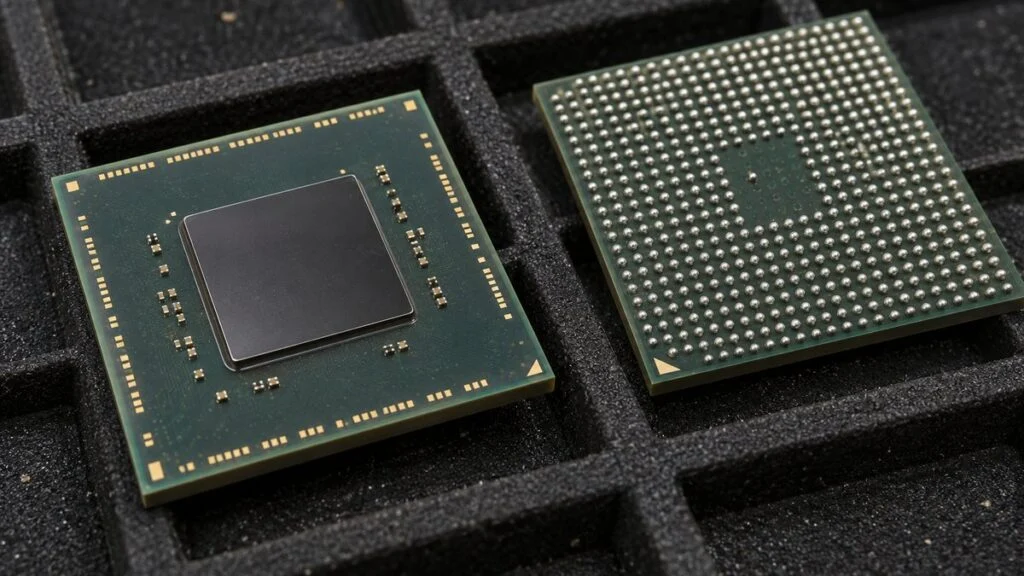
An FC-BGA substrate is the package substrate between a chip and the motherboard. It is used for CPUs, GPUs, AI accelerators, and network chips. Its job is to convert the terminal pitch while carrying signals and power.

A high-performance chip can have thousands to tens of thousands of terminals, spaced about a hair's width apart, and motherboard wiring cannot go that fine. The substrate fans those connections out in stages. "Flip chip" means the chip is mounted face down on tiny bumps, and "BGA" means a grid of solder balls on the underside connects to the board.
Figure 2 shows the layers in a simplified cross section.
The chip's fine terminals spread out inside the substrate before reaching the motherboard.
Layer count and thickness vary by product. Schematic only; not to scale.
The build-up structure alternates copper wiring and insulation on both sides of a core. More layers give more routing paths, which is what lets a substrate carry a large chip with many terminals.
The usual insulator is Ajinomoto Build-up Film (ABF), launched in 1999, with thin grades of about 10 micrometers per layer. Ajinomoto puts its global share in FC-BGA insulation at about 95% and says ABF is used in most high-performance PCs and servers worldwide. You will also see "ABF substrate" in trade press for what suppliers call an FC-BGA substrate.
Terms vary by supplier as well. Shinko calls its product a "flip-chip type package," so confirm that its figures cover the same substrate you are buying.
Mounting the chip and sealing the package is back-end work, and substrate makers sit between material suppliers and that assembly step.
Why AI Substrates Use Up Capacity Faster
Demand is not only a matter of how many substrates are ordered. Each AI substrate is also larger and harder to make, as Figure 3 summarizes.
Each AI substrate is larger and has more layers, so the same line produces fewer of them.
General trends. Actual size and layer count vary by product.
This is why an area-based figure tells you more about load than a count of substrates. In 2024, TOPPAN also cited the production load from larger package substrates as a reason it needed a new site. Counterpoint Research says AI substrates are moving above 100 x 100 mm (about 3.9 x 3.9 in) and from 20-plus to 40-plus layers, with lower yields leaving usable supply below nominal capacity.
Here is a fictional example of the geometry. Suppose a line's capacity is fixed by area, and your package grows from 50 x 50 mm to 100 x 100 mm. Each substrate now takes four times the area, so that line makes at most a quarter as many, before any loss from lower yield or added layers.
How Short Is Supply?
Published estimates agree on the direction but not the size. EDB's statement on the Singapore plant calls advanced substrate capacity a persistent bottleneck. Treat the following as forecasts and press reports, not measured data.
- Counterpoint Research (March 2026): An ABF substrate gap of about 10% in the second half of 2026, widening to about 20% in 2027 before new plants arrive.
- A US brokerage, reported by Taiwan's Economic Daily News (April 2026): Shortfalls of 3% in 2026 and 10% in 2027.
- TrendForce, as reported by 36Kr: ABF substrate lead times of 48–56 weeks, against 12 weeks when supply and demand balance. The article notes this may not apply to every specification or customer.
- Unimicron's chairman (October 2026): Lead times for some key equipment have reached 30 months, and critical materials could fall 20% short in 2027.
The overall market looks calmer than those figures suggest. Figure 4 shows one forecast covering all applications, in which PCs are still the largest at about 40%.
One estimate has the market growing a little under 10% a year.
QYResearch (October 2025, listed by GII). All applications including PCs, not AI alone. Hatched bar is a forecast.
Growth at that pace does not by itself explain a shortage. The likely reading is that tightness is concentrated in large, high-layer-count substrates, where the mix is shifting toward products that are harder to make. Ask about your specific size and layer count, not "FC-BGA" in general.
The Three Expansion Plans in Detail
Each plan below sticks to what the companies or named press outlets have published. Anything not shown here is a question for the supplier.
TOPPAN: Singapore with Broadcom
TOPPAN Holdings held the opening ceremony on September 29, 2026. The operator is Advanced Substrate Technologies (AST), a joint venture of TOPPAN and Broadcom, according to EDB. Trade press names Broadcom as TOPPAN's largest FC-BGA customer.
This is the TOPPAN Group's first FC-BGA plant outside Japan, and EDB describes it as Singapore's first for high-end FC-BGA substrates. The main facts are below.
- Location: Near Jurong Lake District, Singapore
- Size: About 95,000 m² (about 1.02 million sq ft) of total floor area; about 70,000 m² (about 753,000 sq ft) operates in the first phase
- Products: Large, high-layer-count FC-BGA substrates for AI and networking
- Timing: Construction began in March 2024; production is planned for December 2026
- People: 315 employees at the end of September 2026, including more than 200 highly skilled engineers and technicians
- Also planned: R&D functions and training links with local educational institutions
- Not disclosed by the company: Investment amount and equity split, although press reports sometimes give amounts
Read the schedule carefully. Broadcom says the facility came online three months early, but the December 2026 production date is in line with the "end of 2026" start that TOPPAN announced in March 2024. An early building does not tell you when your part will ship.
Figure 5 places Singapore in the longer Niigata story.
Capacity grew at one site in Niigata, and a second site follows in 2026.
Based on TOPPAN Holdings news releases of March 14, 2024, December 17, 2025, and September 30, 2026.
The new Niigata line started in January 2026. TOPPAN says it supports low-dielectric materials and copper surface treatment for high-speed signals, and handles substrates too large for JEDEC-standard trays. Together, the two sites are meant to deliver the FY2027 target.
Ibiden: About ¥500 Billion, Centered on Gifu
In February 2026, Ibiden approved about ¥500 billion of investment in its electronics business for FY2026–FY2028 to expand capacity for high-performance IC package substrates, mainly for servers. Rather than one lump sum, the plan has two parts, both including existing plants overseas. Operation begins in stages from FY2027.
- First part, about ¥220 billion: Gama Plant (Ogaki, Gifu Prefecture) and existing plants. The building was finished in FY2023, and Ibiden decided to invest for volume production after agreeing on a direction with customers.
- Second part, about ¥280 billion: Ono Plant (Ono, Gifu Prefecture) and existing plants, disclosed on February 26, 2026.
Ono is Ibiden's largest domestic site by area, at about 150,000 m² (about 1.6 million sq ft) among eight sites, per the Gifu Shimbun newspaper. It opened on October 10, 2025, with volume production of AI server substrates starting in stages from that month. English sources spell it both "Ono" and "Ohno."
Outside Japan, Ibiden makes IC package substrates in Batangas Province, Philippines, and Penang, Malaysia. Its plan therefore combines large domestic sites with existing overseas plants. Whether your product can be built at those overseas plants is a separate question.
Shinko Electric Industries: Four Plants in Nagano
Shinko is based in Nagano City, and flip-chip type packages are its main product. In October 2021 it announced ¥140 billion for FY2022–FY2025, adding a new site in Chikuma to the Kohoku and Wakaho plants (Nagano City) and the Takaoka Plant (Nakano). The plan was to raise capacity by about 50%, with Chikuma starting in stages from FY2024.
In 2023, Shinko added a separate ¥53.3 billion building at Chikuma for next-generation packages, with operation planned for July 2029. In June 2023, Japan's Ministry of Economy, Trade and Industry certified the plan as a supply-assurance plan under the Economic Security Promotion Act, with a subsidy of up to ¥17.8 billion.
Ownership has changed too. Shinko, formerly a Fujitsu subsidiary, was acquired through a tender offer by JICC-04, a vehicle of JIC Capital, in March 2025 and delisted on June 6, 2025. We found no new capacity target since then, so ask Shinko directly how far the 2021 plan has progressed.
Figure 6 sets the disclosed amounts side by side. Because the periods and scopes differ, it is not a ranking of who is spending the most.
Periods and scopes differ, so amounts are not directly comparable.
Shinko's ¥140 billion and ¥53.3 billion were announced as separate plans and are not added together here. Based on company notices and press reports.
Domestic or Overseas: Explaining Site Risk Internally
If you have to brief management on business continuity planning (BCP) and geopolitical risk, start with the trade-offs. Figure 7 is a general view, not a statement from any of the companies.
Each route has strengths and risks, and each company chooses for its own situation.
A general comparison. For what each company has actually said, see the sections above.
It would be too simple to call TOPPAN the overseas player and the others domestic. These summaries are closer to the facts and can go straight into an internal note.
- TOPPAN: Niigata was its only FC-BGA site, so one investment had to add capacity and a second location. Its 2024 release cites spreading geopolitical and natural disaster risk under a two-site BCP. A customer partner also makes demand at the new site easier to forecast.
- Ibiden: Its new money is centered on two large Gifu sites, using land and buildings it already has, and the plan also covers existing plants overseas.
- Shinko: All four plants named in its plan are in Nagano Prefecture, backed by a government subsidy and a JIC Capital buyout.
TOPPAN has not published a cost or tax comparison explaining why it chose Singapore, so be careful about stating its reasons beyond these. Also remember that a second site gives you little protection until your part number is qualified there.
Japan is also only part of the market. QYResearch names Unimicron, Ibiden, AT&S, Nan Ya PCB, and Shinko among the main makers, with the top five at about 74% of the market. Press reports also describe new investment at Taiwan's Unimicron, Kinsus, and Nan Ya PCB, and an October 2026 partnership between Samsung Electro-Mechanics and NVIDIA on ABF substrates.
What Buyers and Engineers Should Check
The same announcement raises different questions depending on your role.

Figure 8 sorts those questions by what each role can act on.
Start with the card that matches your job.
Material and equipment suppliers should work back from the production start date, because qualification and local support can become conditions of doing business at an overseas site. For buyers, more sites can steady supply, but if the shipping site changes, check for differences in quality and logistics terms.
Checklist Before You Compare Suppliers
Run through these points before a capacity number goes into a sourcing decision.
- Figure: Baseline, end date, product scope, and unit are all identified
- Source: Company statement or press report, and its date
- Fit: Your body size, layer count, and material requirements fall within the capacity being discussed
- Site: The shipping site is named for your part number, not only for the company
- Allocation: Capacity open to you is separated from capacity tied to other customers
- Qualification: Scope, duration, and sample needs are confirmed for each site
- Lead time: A quoted figure exists for your specification, with its assumptions
- Upstream: The supplier has addressed risk in ABF, glass cloth, and other tight materials
- Continuity: The backup route after a disaster or trade restriction is written down
- Logistics: Incoterms, tariffs, and export controls are checked for each shipping site
Questions to Ask a Japanese Substrate Supplier
Published plans will not answer these, so send them early. They work as a written list ahead of a meeting, which also gives the supplier time to circulate them internally.
- Capacity: Does your stated capacity figure use area, units, or another measure? What baseline and product scope does it cover?
- Allocation: How much capacity can be reserved for a customer like us, and from which quarter? What commitment do you need?
- Sites: Which plant would make our part? Can a second plant make it, and is that plant ready today?
- Joint ventures (TOPPAN/AST): Is capacity at the Singapore plant open to customers other than Broadcom, and on what terms?
- Qualification: What does qualifying at a second site involve, how long does it take, and what do you need from us? Would a site transfer trigger a change notification?
- Specifications: What are your current limits for body size and layer count? Do your yield and lead time assumptions change near those limits?
- Lead time: What is the current lead time for our specification, and what is your forecast for the next four quarters?
- Materials: Are ABF film and glass cloth secured for the volumes we are discussing? Are there approved alternatives?
- Continuity: What is your BCP if a plant stops after an earthquake or other disaster? Can you share recovery targets?
Sample Inquiry Email
Adapt this template for a first contact. Fill in the brackets and remove anything your NDA does not allow you to share.
Subject: FC-BGA substrate inquiry: capacity, site, and qualification for [product type]
Dear [Name],
We are evaluating FC-BGA substrate suppliers for [application] with production starting around [quarter/year]. Our outline requirements are below. Further details can follow under NDA.
- Body size: [mm x mm]
- Layer count: [build-up/core]
- Material requirements: [dielectric, others]
- Estimated volume: [units/quarter]
Could you tell us:
- Whether this specification is within your current capability, and at which plant
- Whether a second plant could make it, and when
- How much capacity could be reserved, from when, and under what commitment
- What qualification would require from us, and how long it would take at each plant
- Your current lead time for this specification
If it would be easier, we would be glad to go through these in a call. We would appreciate a first response by [date].
Best regards,
[Name, title, company]
Limits of This Guide
This comparison is a starting point for your questions, not a supplier ranking. Keep these limits in mind.
- It reflects public notices and press reports available on November 2, 2026, and plans can change.
- Some figures come from press reports or market research, and shortage and lead-time estimates vary widely. Your actual allocation and lead time come only from the supplier.
- It covers three Japanese makers. Suppliers in Taiwan, South Korea, and Europe need their own review.
- The trade-offs in Figure 7 and the trends in Figure 3 are general and may not apply to a specific product or plant.
- Export controls, tariffs, and contract terms depend on your product and country. Your legal and trade-compliance teams should decide those.
FAQ
What Does FC-BGA Stand For?
Flip chip ball grid array. The name combines two connection methods: the chip is mounted face down on bumps, and solder balls in a grid on the underside connect to the board.
Who Are the Main FC-BGA Substrate Suppliers?
In Japan, the main makers are TOPPAN, Ibiden, and Shinko Electric Industries. QYResearch's main global names are Unimicron, Ibiden, AT&S, Nan Ya PCB, and Shinko, and press coverage also includes Kinsus and Samsung Electro-Mechanics.
Is There an FC-BGA Substrate Shortage?
Published forecasts say yes for ABF substrates, though the size varies: Counterpoint Research projects about 20% in 2027, while a US brokerage cited in Taiwanese press projects 10%. The tightness appears to be concentrated in large, high-layer-count substrates, so ask about your own specification.
Are TOPPAN's and Ibiden's 2.5x Figures Comparable?
No. TOPPAN's covers its whole FC-BGA business against FY2022, with no unit stated. Ibiden's, reported by Nikkei, covers AI server substrates by area against the current level.
What Is ABF in an FC-BGA Substrate?
ABF is Ajinomoto Build-up Film, an insulating film launched in 1999 that separates the wiring layers in the build-up structure. Ajinomoto puts its global share in FC-BGA insulation at about 95%.
Sources
- Singapore plant opening: TOPPAN Holdings news release (September 30, 2026)
- Joint venture, first-in-Singapore description, supply statement, and Broadcom comment: Singapore Economic Development Board, "AST Completes Singapore's First High-End FC-BGA Substrate Facility"
- Construction start and largest customer: Evertiq, "Broadcom and TOPPAN JV Opens FC-BGA Substrate Plant in Singapore" (September 30, 2026)
- Singapore plan, BCP, and production load: TOPPAN Holdings news release (March 14, 2024, Japanese)
- Niigata new line: TOPPAN Holdings news release (December 17, 2025)
- Niigata mass production from 2014: TOPPAN Holdings news release (December 17, 2025, Japanese)
- Ibiden investment plan: Ibiden notice (February 2026, Japanese)
- Ibiden second part: FilingReader summary of Ibiden's disclosure (February 26, 2026); Logistics Today (February 27, 2026, Japanese)
- Ibiden capacity report: Nikkei (February 2026, Japanese)
- Ono Plant: Evertiq (October 15, 2025); Gifu Shimbun (October 2025, Japanese)
- Ibiden overseas sites: Ibiden notice (September 2022, Japanese)
- Shinko investment plan: Shinko Electric Industries notice (October 4, 2021, Japanese)
- Chikuma building and subsidy: Shinano Mainichi Shimbun (June 2023, Japanese)
- Shinko delisting: Shinko Electric Industries investor page (Japanese); Fujitsu release (January 2025)
- ABF: Ajinomoto, "What Is ABF?" (Japanese)
- Market size and main makers: QYResearch, listed by GII (October 2025, Japanese)
- Substrate size trends and shortage forecast: Counterpoint Research, "From T-Glass Crisis to Capacity Erosion" (March 11, 2026)
- Brokerage shortage forecast: Economic Daily News (April 23, 2026, Chinese)
- Lead times and other suppliers' investment: 36Kr
- Unimicron chairman's comments: TrendForce News (October 20, 2026)
Original article in JapaneseThis guide is adapted from a MONOSCOPE article written for readers in Japan: FC-BGA基板、TOPPANはシンガポールへ|イビデン・新光と増産戦略を比較
About the editor
 MONOSCOPE EditorFOUNDER & EDITOR
Spent about ten years at a plant equipment maker and a plant engineering company, proposing, designing, and commissioning equipment, then moved into web marketing. Now a web consultant for B2B manufacturers, helping them explain their products and technology. Licensed in Japan as an Energy Manager and a Third-Class Chief Electrical Engineer.
Has run an engineering blog since 2017 (500+ articles) and a Japanese YouTube channel with about 20,000 subscribers. Each English guide is written from the Japanese shop-floor point of view and checked against the cited standards.