Fujifilm Expands CMP Slurry Output in Arizona: What It Means
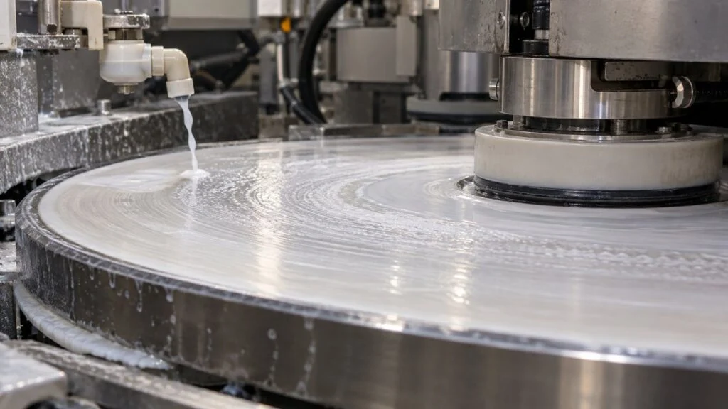
Suppose your Fujifilm account team tells you that some of the copper CMP slurry your fab buys may soon come from Mesa, Arizona, instead of an overseas plant. Before anything ships, you will want to know what actually changed, what Fujifilm has not said yet, and what your qualification and change-control process will need from the supplier.
On October 14, 2026, Fujifilm announced an $18 million (about ¥3 billion) investment in CMP slurry production at its Mesa site. The money covers two things: more capacity for copper interconnect slurry, and new lines that can make many different slurry types. The expanded copper line is scheduled to start in 2027.
This article separates the expansion from the new build, explains how CMP slurry works and where each type is used, looks at why Fujifilm chose Arizona, and ends with a list of questions to ask your CMP slurry supplier.
Location, amount, timing, and scope are public. The size of the capacity increase is not.
Sources: Fujifilm news release (October 14, 2026); Nikkan Kogyo Shimbun (October 15, 2026).
Contents
- What Fujifilm Announced, and What It Did Not
- What Is CMP Slurry?
- CMP Slurry by Process Step: FEOL, MOL, BEOL, and Hybrid Bonding
- Why Arizona?
- Fujifilm's CMP Slurry Plants and Recent Investments
- What US-Made Slurry Means for Your Sourcing
- Questions to Ask Your CMP Slurry Supplier
- Limits of This Article
- FAQ
- Sources
What Fujifilm Announced, and What It Did Not
The investment goes into the Mesa production site of FUJIFILM Electronic Materials U.S.A., Inc., Fujifilm's US semiconductor materials subsidiary. Fujifilm's release describes two separate projects: expanding an existing line and installing new facilities. The $18 million figure is the total for both.
The Expansion: Copper Interconnect Slurry for BEOL
The expansion adds capacity for copper interconnect CMP slurry, which fabs use in back-end-of-line (BEOL) wiring. Fujifilm's release says it holds a leading global market share in this product, and Japanese press coverage puts it at No.
1. The expanded line is scheduled to start operating in 2027.
The New Build: Multi-Product Lines for FEOL, MOL, and Packaging
The new facilities are designed for multi-product manufacturing. They will cover a wide range of slurries for the front end of line (FEOL), where transistors are built, and the middle of line (MOL), the contact layer above them. They will also cover advanced packaging, including hybrid bonding, which joins chips directly to each other.
The release gives no start date for these new facilities. Nikkan Kogyo Shimbun's report describes the whole project as starting in 2027, but Fujifilm's own wording ties 2027 to the expanded copper line only. If your plans depend on a FEOL, MOL, or packaging slurry made in Mesa, ask the supplier for a date in writing.
What Is Still Unknown
Fujifilm calls the new Mesa facilities a bridge that moves technology from the on-site R&D center into volume production. According to Nikkan Kogyo Shimbun, a Japanese industrial daily, the size of the capacity increase has not been disclosed. The same report says the product will ship to customers both inside and outside the US.
No customers have been named. The release also does not include hiring or staffing plans.
What Is CMP Slurry?
Chemical mechanical polishing (CMP), also called chemical mechanical planarization, flattens the wafer surface between process steps. CMP slurry is the polishing liquid used in that step. Fujifilm describes it as a material that evenly flattens semiconductor surfaces where wiring and insulating films of different hardness sit side by side.
How CMP Works
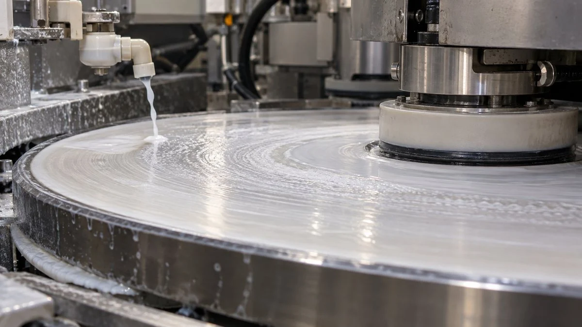
In a CMP tool, slurry flows onto a rotating polishing pad while a carrier presses the silicon wafer face-down against it. Chemicals in the slurry react with the wafer surface, and fine abrasive particles in the liquid remove the reacted material. The result is a combined chemical and mechanical action.
Professor Akira Fukuda of the National Institute of Technology, Tokuyama College, explains that the wafer, the pad, and the slurry interact chemically and mechanically in a very narrow gap. Because these interactions happen on such a small scale and are so complex, slurry improvement has long relied on engineers' experience and intuition.
The figure below shows the basic setup on the polishing table.
Slurry flows onto a rotating pad, and the wafer is pressed against it to flatten the surface.
The wafer is held with the side being polished facing down. Based on research by Professor Akira Fukuda, National Institute of Technology, Tokuyama College.
Why the Surface Must Be Flat
A chip is built by stacking layers of wiring and insulating film on top of the transistors. Each new film leaves small hills and valleys on the surface. If the surface is not flattened before the next layer goes on, the circuits above cannot be patterned accurately.
Fujifilm says its CMP slurry can polish surface topography to within 0.4 nanometers (4 angstroms). To illustrate, the company scales a wafer about 30 cm across up to the size of the Earth: the surface would then stay flat to within about 1.69 cm.
The cycle below repeats for every wiring level in the chip.
Deposit, get topography, polish, and repeat to build up the circuit.
The 0.4 nm figure is the polishing precision Fujifilm states for its CMP slurry (announced August 7, 2026).
A flat surface lets the fab stack more circuitry in the same area. Fujifilm links its slurry directly to the performance of AI chips for that reason: the number of stacked layers and their precision set how much processing a chip can do.
Polishing Soft and Hard Materials at Once
CMP is difficult because soft copper and hard insulating film sit side by side on the same surface. If one material polishes away faster than the other, it leaves a recess; on copper lines this is called dishing. The slurry therefore has to be formulated to balance removal across the different materials.
For its copper slurry, Fujifilm points to three strengths:
- Additives that make the surface easier to polish
- Corrosion inhibitors that protect the copper after polishing
- Technology that keeps abrasive particles evenly dispersed, even at high concentration
All three are formulation choices. A slurry's performance comes from how its abrasive and chemistry are tuned together. That is why the same product made at a new site still deserves a careful look.
CMP Slurry by Process Step: FEOL, MOL, BEOL, and Hybrid Bonding
CMP is not a single step. It appears many times in a wafer's flow, from forming the isolation between transistors to building multilevel interconnects, and each step needs a slurry matched to the material being polished.
Fujifilm's own product pages group its CMP slurries into copper, barrier, cobalt (an emerging interconnect metal), and front-end types for structures such as high-k metal gates. In this announcement, only the copper line for BEOL is being expanded. Front-end, MOL, and packaging grades will be handled together on the new multi-product lines.
The table below maps each process area to what this announcement covers.
BEOL copper is an expansion. Everything else goes on the new multi-product lines.
Process categories follow Fujifilm's news release (October 14, 2026).
Hybrid Bonding: A Newer Use for CMP Slurry
Hybrid bonding joins chips to chips, or wafers to wafers, directly, without solder bumps. If the bonding surface has even slight topography, the copper pads on the two sides will not make proper contact. That makes the final CMP step before bonding critical.
On September 29, 2025, Fujifilm launched a CMP slurry for advanced packaging, developed from its front-end copper interconnect slurry and tuned for surfaces where copper and oxide coexist. The company says a major semiconductor device manufacturer has adopted it for hybrid bonding.
Fujifilm also plans to extend the product to redistribution layers and micro-bumps.
Why Arizona?
Fujifilm's stated reason is AI. Demand for advanced chips is growing fast, and major chipmakers continue to build new and expanded fabs in the US. Nikkan Kogyo Shimbun reports that the expansion is aimed at demand from those new US fabs.
The best-known example is in the same state. On March 3, 2025, TSMC raised its planned Arizona investment to a total of $165 billion, adding three more fabs, two advanced packaging facilities, and a major R&D center.
TSMC had said in January 2025 that its first Arizona fab had begun producing 4 nm chips, and at the time of the March announcement its second fab was under construction for 3 nm and 2 nm technology.
Production Next to the R&D Center
The second reason is that Mesa is home to Fujifilm's global CMP slurry R&D center. Fujifilm says the new multi-product lines are meant to move technologies developed there into volume production quickly.
For leading-edge slurries, tuning the formulation to a customer's process and ramping volume production tend to run as one continuous effort. With development and production at the same site, moving from trial batches to volume supply becomes easier.
The figure below shows the role Fujifilm describes for the Mesa site.
Technology from the R&D center goes into volume production on the new lines and ships inside and outside the US.
Shipping destinations are based on Nikkan Kogyo Shimbun (October 15, 2026). No customers have been named.
Fujifilm's CMP Slurry Plants and Recent Investments
As of February 2025, Fujifilm made CMP slurry at five sites: Arizona in the US; Hsinchu and Tainan in Taiwan; Cheonan in South Korea; and Kikuyo in Kumamoto, Japan. A sixth site in Zwijndrecht, Belgium, was announced that month, with operations scheduled for spring 2026.
The pattern over the past few years is to add capacity in each region where demand grows. Fujifilm tied Kumamoto to AI-related semiconductor demand and Belgium to automotive and industrial chip demand in Europe. The Arizona investment does the same for the US market.
The timeline below lists the main steps.
Japan, Europe, and now the US: capacity is being added region by region.
Based on Fujifilm news releases and reports in EE Times Japan and Kumamoto Nichinichi Shimbun. The Belgium investment also covers photolithography developer.
The business behind these plants has grown quickly. According to EE Times Japan, Fujifilm's CMP slurry sales in fiscal 2024 were 4.9 times those of fiscal 2015, and slurry now makes up about 25% of its semiconductor materials sales.
The figures below describe the slurry business as a whole, not the effect of the Arizona investment.
These describe the overall business, not the impact of this investment.
Source: EE Times Japan (October 7, 2025). Share figures cite a Fuji Keizai market survey. Fujifilm's fiscal year ends in March.
To reach first place overall by fiscal 2030, Fujifilm needs both more volume in copper slurry, where it already leads, and growth in newer uses such as packaging. The Arizona plan appears to pursue both at once: a copper expansion plus new multi-product lines.
What US-Made Slurry Means for Your Sourcing
For a fab or packaging site, a supplier adding capacity nearby can improve supply security, but it does not remove any of your own qualification work. Demand for materials such as CMP slurry tends to rise shortly after new fabs are built, and it continues for years. Here is how the announcement plays out for process, purchasing, and supplier-quality teams.
Shorter Supply Lines, Same Qualification Burden
Local production can shorten transit and reduce exposure to ocean freight and border delays. A slurry made at a new site, or on a new line, is still a change your fab will want to evaluate. Check your supply agreement: a change of manufacturing site is typically handled as a product change notification (PCN) and can trigger requalification on your tools.
Ask early whether your current part number will be made in Mesa, stay at its current site, or be produced at both. Each answer leads to a different plan for wafer trials, data review, and cutover.
Dual Sourcing Within One Supplier
Fujifilm makes slurry in the US, Taiwan, South Korea, and Japan, with Belgium scheduled to join. If the same formulation can be qualified at two of those sites, you gain a second source without changing suppliers. That only works if both sites are qualified on your process and the supplier commits to keeping them aligned.
Lot-to-Lot Consistency and Local Technical Support
A supplier's overseas site has to do more than blend and fill. It needs engineers who can tune formulations to your process and a quality system that ensures each lot meets specifications.
The closer a site links development and production, as Mesa now aims to do, the more of that work happens locally. Fujifilm has not announced hiring plans, so ask who will support your fab day to day.
Outside the US
Mesa product is expected to ship outside the US as well, so fabs and packaging sites in Asia may see it in their supply chain. Fujifilm also announced in September 2026 a separate investment of about $83 million in its first semiconductor materials plant in India, starting with front-end process chemicals. That plant is not a CMP slurry announcement, and reports give fiscal 2028 for commercial production.
Questions to Ask Your CMP Slurry Supplier
Use the list below when your supplier proposes product from a new site or line, whether that is Fujifilm's Mesa plant or any other. Adapt the wording to your own qualification procedure.
Site and Schedule
- Will our current part number be produced in Mesa, at its current site, or at both?
- When will the expanded copper line ship qualified product, and when will the new multi-product lines start?
- Which slurry types (copper, barrier, front end, hybrid bonding) will each line make?
- Will raw materials, especially the abrasive, come from the same sources as the currently qualified product?
Qualification and Change Control
- Is the Mesa process a copy of the qualified site's process (often called copy-exact), or are there differences in equipment, recipe, or raw materials?
- What data will you provide for qualification: certificate of analysis (CoA) comparisons, particle data, and wafer-level polishing results?
- Will the site change be issued as a formal PCN, and how much notice will we get before cutover?
- Can we run qualification lots from the new line in parallel with current supply?
Lot-to-Lot Variation
- Which parameters appear on the CoA (for example, particle size distribution, large-particle counts, pH, abrasive concentration, metals), and what are the limits?
- Can you share statistical process control data across recent lots, and will the same limits apply at both sites?
- How do you trace a lot back to its raw-material batches if we see a defect excursion?
Logistics and Support
- What lead time and safety stock do you plan for our fab from Mesa compared with today?
- What are the shelf life, storage temperature range, and packaging (drum, tote, bulk) for the product?
- Who provides on-site technical support, and is there a local contact for failure analysis?
- If one plant goes down, which other site can supply our qualified product, and how fast?
Limits of This Article
This article is based on Fujifilm's public announcements and press coverage up to early November 2026. It does not cover capacity numbers or customer names, because neither has been published.
- Start dates, product scope, and site assignments can change. Confirm them with the supplier.
- Share figures come from a Fuji Keizai survey cited in press coverage. Fujifilm's Arizona release itself gives no share number.
- How a site change is handled (PCN, requalification depth, notice period) depends on your supply agreement and your fab's procedures, not on this article.
FAQ
How Much Is Fujifilm Investing in Arizona CMP Slurry Production?
$18 million (about ¥3 billion). That total covers both the copper slurry expansion and the new multi-product facilities. Fujifilm has not said by what percentage capacity will grow.
When Will the New Arizona Lines Start?
The expanded copper interconnect slurry line is scheduled to start in 2027. Fujifilm's release gives no start date for the new multi-product lines for FEOL, MOL, and advanced packaging.
What Is the Difference Between CMP Slurry and a CMP Pad?
The slurry is the liquid that carries the abrasive particles and chemicals. The pad is the surface on the rotating table that the wafer is pressed against. CMP needs the wafer, the pad, and the slurry working together, so neither consumable can polish on its own.
What Is a Post-CMP Cleaner?
A post-CMP cleaner washes the wafer after polishing. It removes particles, trace metals, and organic residues while protecting the metal surface. Fujifilm sells post-CMP cleaners alongside its slurries and offers both together.
Why Does Hybrid Bonding Need a Special CMP Slurry?
Because the bonding surface mixes copper pads and oxide, and the two sides only bond properly if that surface is extremely flat. Fujifilm's hybrid bonding slurry, launched in September 2025, adjusts additives, corrosion inhibitors, and abrasives for that mixed surface.
Sources
- Arizona investment, scope, timing, and R&D center: Fujifilm, "Fujifilm to Expand CMP Slurry Production Capacity in the United States" (October 14, 2026)
- Undisclosed capacity increase and shipping destinations: Nikkan Kogyo Shimbun via Newswitch (October 15, 2026, Japanese)
- Arizona investment coverage: EE Times Japan (October 16, 2026, Japanese)
- Hybrid bonding slurry launch: Fujifilm, CMP slurry for advanced packaging (September 29, 2025)
- 0.4 nm polishing precision: Fujifilm, corporate TV commercial on semiconductor materials (August 7, 2026, Japanese)
- Sales growth, share, and 2030 targets: EE Times Japan, Fujifilm CMP slurry growth strategy (October 7, 2025, Japanese)
- CMP slurry product types: Fujifilm, CMP slurries product page
- How CMP works: Akira Fukuda, National Institute of Technology, Tokuyama College, research on semiconductor device polishing (Japanese)
- Kumamoto plant announcement: EE Times Japan (September 9, 2022, Japanese)
- Kumamoto capacity increase: Kumamoto Nichinichi Shimbun (December 5, 2024, Japanese)
- Belgium investment and CMP slurry production sites: Fujifilm, "Fujifilm to Invest 4 Billion yen in Belgium for CMP Slurries and Photolithography-related Materials" (February 5, 2025)
- TSMC Arizona investment: Greater Phoenix Economic Council, "TSMC announces $100 billion investment for fabs, packaging and R&D in Arizona" (March 2025)
- India semiconductor materials plant: Evertiq, "Fujifilm to invest $83M in semiconductor materials facility in India" (September 17, 2026)
Original article in JapaneseThis guide is adapted from a MONOSCOPE article written for readers in Japan: 富士フイルムが米アリゾナでCMPスラリー増強|半導体の研磨材が要る理由
About the editor
 MONOSCOPE EditorFOUNDER & EDITOR
Spent about ten years at a plant equipment maker and a plant engineering company, proposing, designing, and commissioning equipment, then moved into web marketing. Now a web consultant for B2B manufacturers, helping them explain their products and technology. Licensed in Japan as an Energy Manager and a Third-Class Chief Electrical Engineer.
Has run an engineering blog since 2017 (500+ articles) and a Japanese YouTube channel with about 20,000 subscribers. Each English guide is written from the Japanese shop-floor point of view and checked against the cited standards.