MLCC Manufacturing Process: Why Japanese Makers Lead
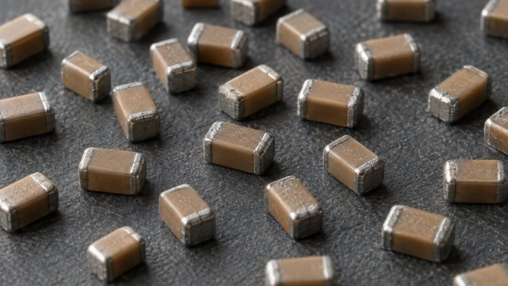
If you buy or design with multilayer ceramic capacitors (MLCCs), you have probably seen the same few names on most of your bills of materials: Murata, TDK, and Taiyo Yuden from Japan, plus Samsung Electro-Mechanics from Korea. When AI-server demand tightens supply, as it did in 2026, the question comes up fast: why can't another supplier simply make more?
The answer is in how MLCCs are made. A chip the size of a grain of rice can hold several hundred to more than 1,000 alternating layers of ceramic and metal, and each ceramic layer is anywhere from under 1 µm to a few µm thick. Getting there takes tight control of everything from the starting powder to the firing furnace, which is why world supply is concentrated in a small group of makers led by Japanese companies.
This guide walks through the MLCC structure and types, the 10-step manufacturing process, and why thinner layers mean more capacitance. It then covers why Japanese makers lead, what the AI-server boom means for supply, and what to check when you source or substitute MLCCs from Japanese suppliers.
- An MLCC is a chip capacitor made by stacking several hundred to more than 1,000 layers of dielectric ceramic and internal electrodes, then firing the stack
- The manufacturing process has 10 steps in three stages: materials (powder blending, slurry, sheet casting), printing and stacking (electrode printing, stacking, pressing, cutting), and firing and finishing (binder burnout and firing, terminations and plating, inspection and packaging)
- Capacitance goes up when layers get thinner and more numerous, but thinner sheets turn small defects and firing distortion into failures
- Japanese makers lead because they pioneered nickel electrodes, have materials suppliers close at home, and build much of their own production equipment
- Japanese datasheets often use metric size codes: a Japanese "1005" is the US "0402"
Contents
- What Is a Multilayer Ceramic Capacitor (MLCC)?
- MLCC Types, Size Codes, and Typical Counts
- MLCC Manufacturing Process: 10 Steps From Powder to Chip
- Why Thinner Layers Mean More Capacitance
- Why Japanese Makers Lead in MLCCs
- AI Servers and the MLCC Supply Squeeze
- What This Means When You Source MLCCs From Japanese Makers
- FAQ
- Sources
What Is a Multilayer Ceramic Capacitor (MLCC)?
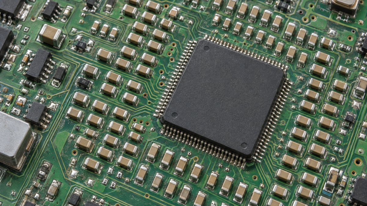
A capacitor stores electric charge and releases it when the circuit needs it. Because it blocks DC and passes AC, designers use it to shunt unwanted noise and smooth out supply-voltage fluctuations.
When an IC switches, its current draw changes suddenly and the supply voltage dips for an instant. A capacitor placed nearby supplies that current right away and keeps the circuit running stably. That is why almost every semiconductor in a smartphone, car, or server has capacitors next to it.
Capacitors come in several types, including electrolytic and film. An MLCC (multilayer ceramic capacitor) uses ceramic as its dielectric, the insulator that stores the charge, and builds it up in layers. Compared with electrolytic capacitors, MLCCs are smaller and have lower equivalent series resistance (ESR) and equivalent series inductance (ESL), which makes them a good fit around the power pins of fast-switching chips.
Structure: A Stack of Dielectric and Electrodes
The simplest capacitor is a dielectric sandwiched between two electrodes. An MLCC stacks that unit many times over to increase the area where the electrodes face each other.
Every other internal electrode runs out to the left end of the chip, and the rest run to the right end, where they connect to the external terminations. The result is several hundred to more than 1,000 capacitors connected in parallel, which is how an MLCC packs high capacitance into a tiny volume.
Dielectric layers and internal electrodes alternate, and the external terminations on each end connect them in parallel.
Note: The number of layers is reduced for clarity. Real parts range from a few layers to more than 1,000.
MLCC Types, Size Codes, and Typical Counts
Two MLCCs can look identical and behave very differently, depending on the dielectric material and the size. Whether you design the circuit or read the purchase specification, start with these two points.
Class 1 vs. Class 2 Dielectrics
MLCCs fall into two broad groups by dielectric: Class 1 (low permittivity) and Class 2 (high permittivity).
Class 1 parts use materials such as calcium zirconate. Their capacitance is small, but it barely changes with temperature, which is why they are also called temperature-compensating capacitors.
Class 2 parts use barium titanate, a ferroelectric material. Its relative permittivity (a measure of how much charge a material can store) runs from the low thousands to about 12,000, so makers can build small, high-capacitance parts. The trade-off is that capacitance shifts with temperature and applied voltage, so designers need to check the capacitance under actual operating conditions.
The choice comes down to stability or capacitance.
Note: JIS and EIA define and name temperature characteristics differently. The reference temperature for capacitance change is 20°C in JIS and 25°C in EIA.
Rated voltage is the other spec you cannot skip. MLCCs are available from 2.5 V up to the tens of kilovolts. A higher voltage rating needs a thicker dielectric layer, so at the same size you get less capacitance, and at the same capacitance you need a bigger chip.
Size Codes: Metric on Japanese Datasheets, Inch in the US
MLCC sizes are named with a four-digit code that combines length and width. Japanese makers and many Japanese documents use the metric (mm) code: "1005" means 1.0 mm × 0.5 mm, and "0603" means 0.6 mm × 0.3 mm. Datasheets aimed at US customers usually lead with the EIA inch code, and the same digits can mean different parts. A metric 0603 is an inch 0201, while an inch 0603 is a metric 1608. When a drawing or BOM from Japan lists a size, confirm which system it uses.
| Metric code (mm) | Dimensions (L × W) | EIA inch code |
|---|---|---|
| 1608 | 1.6 × 0.8 mm | 0603 |
| 1005 | 1.0 × 0.5 mm | 0402 |
| 0603 | 0.6 × 0.3 mm | 0201 |
| 0402 | 0.4 × 0.2 mm | 01005 |
| 0201 | 0.25 × 0.125 mm | 008004 |
| 016008 | 0.16 × 0.08 mm | 006003 |
In the 2000s, the mainstream sizes were 1608 and 1005 (metric). As devices shrank and part counts rose, the mainstream shifted to metric 0603 around 2018. Mass production of the metric 0201 size (0.25 mm × 0.125 mm) started in 2014, and in September 2024 Murata announced a 0.16 mm × 0.08 mm part (metric 016008, inch 006003). Murata puts its volume about 75% below that of the previous smallest size, metric 0201.
By length, the mainstream size has shrunk by more than half in about 20 years.
Note: Bars show length relative to the 1608 size (1.6 mm = 100). Bold codes are metric (mm).
How Many MLCCs Go Into One Device
A single device uses anywhere from several hundred to tens of thousands of MLCCs. According to an article by the Ceramic Society of Japan, a high-end smartphone uses about 1,300 and an electric vehicle about 10,000.
5G smartphones need circuits for each additional frequency band, so their MLCC count went up. Cars follow the same pattern: the more electrification and automated-driving functions they carry, the more electronic parts they need, and MLCCs are often cited as a part that grows with the shift to EVs.
MLCC Manufacturing Process: 10 Steps From Powder to Chip
In outline, the process is simple: turn ceramic powder into a liquid, cast it into thin sheets, print electrodes on them, stack, cut, and fire. In practice, the material changes state and undergoes chemical reactions along the way, so every step depends on accumulated know-how.
The process falls into three stages: materials, forming and stacking, and firing and finishing.
Note: Step names and boundaries vary by maker and product.
Powder and Slurry
Everything starts with the dielectric powder. For Class 2 parts, barium titanate is the main ingredient, with additives that tune its properties. The more uniform the particle size and shape, the easier it is to form thin, even layers later on.
The powder is mixed with organic solvent, binder (a resin that holds the particles together), and dispersant to make a fluid slurry. The particles must be evenly dispersed, but mixing too hard chips the particles and degrades quality, so tuning the dispersion conditions takes real skill.
Sheet Casting (Green Sheets)
The slurry is coated thinly onto a carrier film such as PET and dried. Because the sheet has not yet been fired, it is called a green sheet. The thinner the sheet, the more directly any voids, surface roughness, or pinholes turn into defects.
The carrier film itself must be extremely smooth. Makers use films developed specifically for MLCCs, such as Toray's release-coated polyester film.
Electrode Printing
Internal-electrode paste is printed onto the green sheet in a pattern, by screen printing or similar methods. One print lays down the electrodes for many chips at once.
The paste is fine nickel powder mixed with solvent and binder. Yield on thin-layer parts depends on printing thin, sharply defined rectangular electrode patterns without bleeding or gaps.
Stacking, Pressing, and Cutting
Hundreds of printed sheets are stacked, with the electrode pattern shifted left or right on each sheet. That offset is what makes alternate internal electrodes reach opposite ends of the chip.
The stack is pressed into a single laminated bar holding many chips, and a cutting machine slices it into individual pieces. At this stage, the material is not yet ceramic; it is soft, much like modeling clay. The angle and condition of the cutting blade directly affect the quality of the cut faces.
Binder Burnout and Firing
The cut chips are first heated to remove the organic content of the sheets and electrode paste (binder burnout). They are then fired at about 1,000–1,300°C, which sinters the powder into ceramic. Because the dielectric and electrodes are fired together, the heating profile and furnace atmosphere have a large effect on quality.
With nickel electrodes, firing in air would oxidize the metal. Makers therefore fire in a reducing atmosphere with little oxygen, but that creates a new problem: the barium titanate is reduced, which degrades its insulation. The fix was reduction-resistant dielectric materials that keep their properties in a reducing atmosphere.
NGK Insulators, which also builds firing furnaces, lists four thermal processes for MLCCs:
- Primary and secondary binder burnout
- Sintering
- Reoxidation
- Termination firing
These steps require precise control of not only temperature but also oxygen partial pressure, hydrogen concentration, and dew point.
Terminations, Plating, and Inspection
After firing, the ends of the internal electrodes are exposed on both ends of the chip. Metal paste is applied there and fired to form the external terminations, which tie together the electrodes on each side.
The terminations are then plated with nickel and tin so the chip can be soldered to a board.
Finally, the chips are tested for electrical characteristics and appearance, then packaged and shipped. With huge volumes of parts smaller than 1 mm, automated image-based inspection is essential, and electronic-component plants now also use methods such as AI visual inspection.
Why Thinner Layers Mean More Capacitance
Getting more capacitance out of the same chip size is the main goal of MLCC development. The parallel-plate capacitance formula shows why.
To raise capacitance, increase the numerator or shrink the denominator.
Note: Internal-electrode thickness is not in the formula, but thinner electrodes also let more layers fit into the same height.
In the formula, relative permittivity is largely fixed by the material, and electrode area is capped by chip size. So in practice, development has focused on thinning the dielectric and adding layers. A thinner dielectric raises the capacitance of each layer and lets more layers fit into the same height, so the gain is doubled.
What Gets Harder as Layers Get Thinner
Thinner layers raise the difficulty of every other step. Once the dielectric is sub-µm thick, slight powder agglomeration, surface roughness, or a pinhole in the sheet can directly cause a short circuit or insulation failure.
Makers respond with fine powders of uniform particle size, dispersants and binders that lay those particles down evenly, and smooth carrier films. The electrode side needs the same care: finer nickel powder and printing that does not bleed. Yield improves only when materials, equipment, and process conditions are optimized together, and that is what makes MLCCs hard to make.
Examples With More Than 1,000 Layers
Thinner, more numerous layers have pushed MLCCs into territory once held by electrolytic capacitors. In 2018, an MLCC with more than 1,000 layers in the metric 4532 size (4.5 mm × 3.2 mm) reached 1,000 µF and went into mass production, making all-ceramic power-supply capacitor designs increasingly possible.
Small parts follow the same trend. In July 2025, Murata began mass production of a 47 µF MLCC in the metric 1005 size (1.0 mm × 0.5 mm; inch 0402) at a plant in Fukui Prefecture. Murata says it achieved about twice the capacitance of its previous part by forming more than 1,000 thin, uniform ceramic layers.
Why Japanese Makers Lead in MLCCs
The main MLCC makers are Murata Manufacturing, TDK, and Taiyo Yuden from Japan, along with Samsung Electro-Mechanics from Korea and others. Published share figures are rough and rarely give a year, so read the table below as an indication of scale, not a ranking you can cite to the decimal point.
| Maker or group | Share of the global MLCC market | Period | Source |
|---|---|---|---|
| Murata Manufacturing (Japan) | 40% | No year given (Murata's capacitor business page, checked October 2026) | Murata, company figure |
| Samsung Electro-Mechanics (Korea) | 24%, second to Murata | First half of 2024 | Passive Components Blog (June 2025), research firm not named |
| Mainland Chinese makers combined | About 10% of revenue | Second half of 2024 | Passive Components Blog (June 2025), citing Korean and Chinese media |
Murata calls itself the world's No. 1 MLCC supplier, and Japanese makers have long been at the center of the market. For how MLCCs compare with Japan's other top-share products, see Where Japan Holds Top Global Share: Materials and Equipment.
A long history alone does not explain the lead. The bigger factor appears to be a way of working that improves materials, process, and equipment together, which suits a product like the MLCC.
Accumulated technology, materials, equipment, and quality reinforce one another.
Pioneering Nickel Electrodes
Early MLCCs used precious metals such as palladium for the internal electrodes. Those metals are expensive, and the electrode cost rises with every layer added.
Switching to low-cost nickel was the obvious goal, but it ran into the problem described above: firing in a reducing atmosphere degrades the dielectric. According to the Japan Institute of Invention and Innovation's list of 100 postwar Japanese innovations, Japanese companies were the ones that solved it. Nickel cut materials cost and laid the groundwork for more layers and higher capacitance.
Japanese companies built it up step by step, from materials research to mass production and reliability.
Note: Based on the Japan Institute of Invention and Innovation's list of 100 postwar Japanese innovations.
Materials Suppliers Close at Home
Much of an MLCC's quality is decided at the raw-material stage. For barium titanate, the main dielectric ingredient, Sakai Chemical Industry makes high-purity, uniform particles, mainly by hydrothermal synthesis. For electrode nickel powder, Sumitomo Metal Mining has developed ultrafine powder of 0.1 µm or less with its own wet process.
For the release film used in sheet casting, Toray announced in October 2022 that it would raise production capacity for its Lumirror MLCC film at its Gifu plant to 1.6 times the existing level. The investment was JPY 8 billion, with operation scheduled for 2025.
Working closely with upstream makers of powders, pastes, and films to improve materials together is a major strength for Japanese MLCC makers. MLCCs are also a leading fine-ceramics product, and the idea of firing raw materials into a product links them to Japan's wider ceramics industry, which includes glass and cement.
Vertical Integration Down to the Equipment
Murata describes its approach as a vertically integrated production system that keeps critical parts of the process in-house, from materials to finished products.
A 2019 Nikkei report from inside Izumo Murata Manufacturing described almost all of the plant's production equipment as developed and built in-house. A group company makes the screens for electrode printing, and the cutting blades are sharpened in-house, with the angle changed for each product.
Because MLCCs depend on such a tangle of materials, process conditions, and equipment, a maker that buys equipment off the shelf hits the same limits as competitors using the same machines. A maker that builds its own can rework the equipment as its materials improve, and the know-how stays inside the company.
AI Servers and the MLCC Supply Squeeze
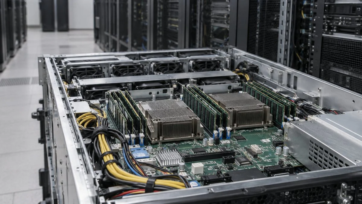
In recent years, AI servers have been the fastest-moving part of the MLCC market. The GPUs used to train and run generative AI draw a lot of power, and stabilizing that power takes an enormous number of capacitors.
An AI server is said to use more than 10 times as many MLCCs as a standard server.
Note: Smartphone and EV figures are from the Ceramic Society of Japan (2022). Server figures are Samsung Electro-Mechanics' estimates as reported by Denshi Device Sangyo Shimbun (October 2025). The same paper also gave 1,800–2,500 for standard servers and 10,000 to more than 20,000 for AI servers, so counts vary by model and configuration.
Why GPUs Need So Many Capacitors Nearby
At its April 2026 earnings briefing, Murata explained that server capacitors go into power-supply circuits. Higher-voltage parts sit at the power input, while small, high-capacitance, low-voltage parts sit close to the GPUs and TPUs, and demand for both is growing.
Higher-performance chips draw more current, and their current draw fluctuates more sharply. As advanced packaging, such as putting a GPU and memory in one package, pushes performance up in back-end semiconductor processing, the power-delivery parts around the chip matter more. Designs increasingly place power circuits right next to the main chips, and Taiyo Yuden, for example, offers MLCCs that can be embedded in the circuit board.
Related: Semiconductor Back-End Process: Flow and Japanese Suppliers
At the same briefing, Murata also noted that because GPUs are surrounded by so many capacitors, even small capacitance differences could cause malfunctions. This market rewards not just volume but tight part-to-part consistency.
Recent Moves by Japanese Makers
Murata reported record revenue of JPY 1,830.9 billion for fiscal 2025 (year ended March 2026), with data-center-related sales up about 74% from the year before. It expects data-center sales to grow 84% in fiscal 2026, and its MLCC orders are well ahead of shipments, with a book-to-bill ratio of 1.36.
To keep up, Murata decided on an additional JPY 80 billion investment to raise output, mainly of server MLCCs. According to Nikkan Kogyo Shimbun, the plan puts about JPY 40 billion into each of fiscal 2026 and 2027 to raise production capacity by 10–15% from the current level. In April 2026, Murata also completed a 10-story production building in Izumo, Shimane Prefecture, a JPY 47 billion investment.
Other makers are moving too:
- Taiyo Yuden: began mass production of a 22 µF part in the metric 1005 size, designed for embedding in circuit boards, in September 2025
- Taiyo Yuden: began mass production of a new server part with about five times the capacitance of its previous product, at a plant in Gunma Prefecture, in November 2025
- TDK: announced a 100 V-rated part in the metric 1608 size in June 2025
Murata describes data-center demand as a market where securing supply matters more than price, and it sees only a limited number of makers able to supply it. It has also said it cannot yet fully predict how far demand will grow, so the makers themselves are cautious about how long the boom will last.
To see the whole MLCC supply chain, look beyond the capacitor makers to the upstream and supporting companies: makers of dielectric powder, nickel powder, release film, firing furnaces, and inspection equipment. In AI-server power supplies, demand is also growing for SiC and GaN power semiconductors.
What This Means When You Source MLCCs From Japanese Makers
The process explains the supply picture. Adding capacity relies on matched materials and in-house equipment, and a part that looks identical on paper may not perform the same way in your circuit. The checklist below covers what to confirm before you approve a part, add a second source, or accept a substitute.
MLCC Sourcing Checklist
| Item | What to check | Why it matters |
|---|---|---|
| Size code | Is the size metric (e.g., 1005) or EIA inch (e.g., 0402)? | The same digits can mean different chips (metric 0603 = inch 0201) |
| Temperature characteristic | Code (C0G, X7R, X5R, etc.) and whether it is a JIS or EIA definition | Reference temperature differs (JIS 20°C, EIA 25°C) |
| Capacitance under bias | Effective capacitance at your DC voltage and temperature (Class 2) | Class 2 capacitance shifts with voltage and temperature |
| Rated voltage | Rated voltage vs. your circuit; size needed for that rating | Higher ratings need thicker layers, so less capacitance per size |
| Grade and qualification | Automotive or other high-reliability grade, and what qualification the maker states | General-purpose and automotive parts can share a size and value but not a grade |
| Lead time and allocation | Current lead time, allocation status, and order cover | High-capacitance, small-size parts for AI servers are where demand is tightest |
| Change notices | How the maker announces process, material, or plant changes | Capacity expansions often mean new lines or plants |
| Substitutes | Whether a cross-referenced part from another maker has been checked in your circuit | Matching nominal specs does not guarantee the same behavior |
Sample Inquiry to a Japanese Supplier or Distributor
Short, numbered questions get faster and clearer answers from Japanese suppliers and their distributors. Adapt this example (the part number is fictional):
Subject: Inquiry on MLCC part number ABC1005X5R106 (example)
Hello,
We are evaluating the part above for a new design. Could you confirm the following?
1. Is the size code metric (1.0 × 0.5 mm) or EIA inch?
2. Is the temperature characteristic defined by JIS or EIA?
3. Can you share the DC bias and temperature characteristic curves?
4. Is there an automotive or high-reliability grade of this part, and what qualification applies?
5. What are the current standard lead time and allocation status?
6. How will you notify us of any process, material, or production-site changes?Thank you for your help.
Best regards,
Limits of This Guide
The 10 steps describe the general flow. Step names, order, and conditions vary by maker and product, and makers rarely publish detailed process conditions. Share figures come from different sources and periods, and most do not say whether they measure revenue or units. Device MLCC counts are estimates that vary by model. For part selection and qualification, follow the maker's datasheet and your own design and quality rules, and confirm lead times directly with the supplier.
FAQ
What Does MLCC Stand For?
MLCC stands for multilayer ceramic capacitor (in Japanese, 積層セラミックコンデンサ, sekiso seramikku kondensa). The name describes the structure: ceramic dielectric layers stacked alternately with internal electrodes.
How Is an MLCC Different From an Electrolytic Capacitor?
An MLCC is smaller and has lower ESR and ESL, so it suits the power circuits around fast-switching chips. With thinner, more numerous layers, high-capacitance MLCCs are now mass-produced and are moving into applications that electrolytic capacitors used to cover.
Which Companies Have the Largest MLCC Market Share?
Murata Manufacturing leads; its own figure is 40% (no year stated). Samsung Electro-Mechanics was second at 24% in the first half of 2024, according to a June 2025 industry report. TDK and Taiyo Yuden from Japan are among the other major makers, and mainland Chinese makers together reached about 10% of revenue in the second half of 2024.
Is There an MLCC Shortage in 2026?
Demand from AI servers has surged, and supply is tight for some parts. Murata reports MLCC orders well ahead of shipments (book-to-bill 1.36) and is investing an additional JPY 80 billion, mainly in server MLCCs. It describes data-center customers as prioritizing supply over price but says it cannot yet fully predict how far demand will grow.
Is a Japanese "1005" MLCC the Same as a US "0402"?
Yes. Metric 1005 (1.0 mm × 0.5 mm) is the same size as EIA inch 0402. Check the system every time, because the same digits can refer to different sizes: metric 0603 is inch 0201.
Sources
- Structure, materials, process, MLCC counts, size history: Ceramic Society of Japan, "Ceramics" Vol. 57 (2022) No. 12, "Multilayer Ceramic Capacitors" (Japanese)
- Firing temperature and plating: EDN Japan, "How multilayer ceramic chip capacitors are made" (Japanese)
- Temperature characteristic codes: IR Engineer Education Institute, "MLCC basics" (Japanese)
- History of nickel electrodes: Japan Institute of Invention and Innovation, "100 Postwar Japanese Innovations: Multilayer Ceramic Capacitors" (Japanese)
- Thermal processes and atmosphere control: NGK Insulators, "Firing furnaces for the MLCC manufacturing process" (Japanese)
- Murata's MLCC market share (40%): Murata Manufacturing, "Capacitors" business page
- Samsung Electro-Mechanics and Chinese makers' shares: Passive Components Blog, "China's MLCC Makers Reach 10% Market Share" (June 2025)
- Vertically integrated production: Murata, "Production technology" (Japanese); Murata, "Strengths of Murata capacitors" (Japanese)
- In-house equipment at Izumo Murata: Nikkei, report from Murata's plant (June 4, 2019) (Japanese)
- 0.16 mm × 0.08 mm MLCC: EE Times Japan (September 25, 2024) (Japanese); Murata news release (September 19, 2024)
- 47 µF in 1.0 mm × 0.5 mm: Murata news release (July 10, 2025); Nikkei (July 14, 2025) (Japanese)
- Results, data-center demand, investment: Murata, FY2025 earnings briefing (April 30, 2026) (Japanese)
- JPY 80 billion additional investment: Newswitch (Nikkan Kogyo Shimbun) (Japanese)
- New production building in Izumo: Nikkei (April 3, 2026) (Japanese)
- Server MLCC counts and new products: Denshi Device Sangyo Shimbun (October 3, 2025) (Japanese)
- Taiyo Yuden's new server part: Nikkei (December 2, 2025) (Japanese)
- Release film capacity: Toray, Lumirror MLCC release film capacity increase (October 7, 2022) (Japanese)
- Barium titanate: Sakai Chemical Industry, "Electronic materials" (Japanese)
- Ultrafine nickel powder: Sumitomo Metal Mining X-MINING, "Ultrafine nickel powder" (Japanese)
Original article in JapaneseThis guide is adapted from a MONOSCOPE article written for readers in Japan: 積層セラミックコンデンサ(MLCC)の製造工程|作り方10ステップと日本メーカーが強い理由
About the editor
 MONOSCOPE EditorFOUNDER & EDITOR
Spent about ten years at a plant equipment maker and a plant engineering company, proposing, designing, and commissioning equipment, then moved into web marketing. Now a web consultant for B2B manufacturers, helping them explain their products and technology. Licensed in Japan as an Energy Manager and a Third-Class Chief Electrical Engineer.
Has run an engineering blog since 2017 (500+ articles) and a Japanese YouTube channel with about 20,000 subscribers. Each English guide is written from the Japanese shop-floor point of view and checked against the cited standards.