Semiconductor Back-End Process: Flow and Japanese Suppliers
Walk through an assembly-and-test line in Malaysia, the Philippines, Vietnam, India, or the US and look at the nameplates. The dicing saws and grinders, the testers at the end of the line, and many of the films and resins on the material list are likely to come from Japan. Japan builds relatively few of the chips themselves, but it supplies a large part of the equipment and materials that turn wafers into finished packages.
This guide explains the semiconductor back-end process step by step, from wafer test to final test. It also covers why advanced packaging for AI chips has become a priority, where Japanese equipment and materials suppliers sit at each step (with the share each company publishes, its basis, and its date), and what to ask a Japanese supplier before you qualify a new tool or material.
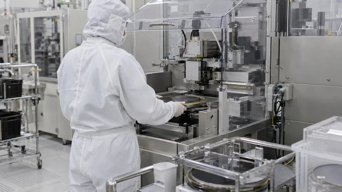
Contents
- What Is the Semiconductor Back-End Process?
- Back-End Process Flow, Step by Step
- Where Japanese Suppliers Sit in the Back End
- Main Semiconductor Package Types
- How Chips Connect: Wire Bonding, Flip Chip, and Hybrid Bonding
- What Is Advanced Packaging?
- Why Advanced Packaging Matters Now
- Who Does Back-End Work: OSATs, Foundries, and Japan
- Advanced Packaging Projects in Japan
- Questions to Ask a Japanese Back-End Supplier
- Limits of This Guide
- FAQ
- Sources
What Is the Semiconductor Back-End Process?
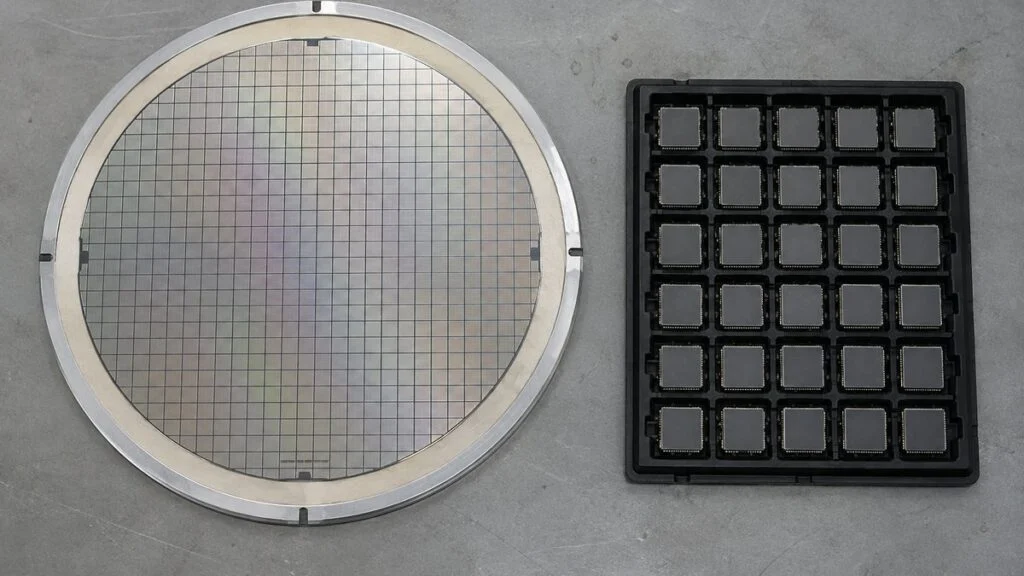
Chipmaking splits into two halves. The front end builds circuits on a wafer, a thin silicon disc. The back end cuts that wafer into individual chips and turns each one into a component that can be mounted on a circuit board. In Japanese, the two halves are called mae-kotei (前工程, front-end process) and ato-kotei (後工程, back-end process), and you will see these terms in Japanese supplier documents.
A bare chip is easily damaged by moisture, shock, and static electricity, and it cannot be soldered to a board as it is. The back end places it in a package: a protective housing with terminals that connect it to the outside world.
Along the way, the back end controls chip thickness in steps of tens of micrometers, connects chips with wires finer than a human hair or with tiny metal bumps, and tests every part before it ships. It has two main parts. Assembly thins the wafer, cuts it into chips, attaches each chip to a lead frame or substrate, connects it electrically, and seals it in resin. Test checks that each finished device works to specification so that only good parts ship.
The front end builds the circuits. The back end turns them into parts you can use.
In advanced packaging, a fifth job is added: combining several chips into one package to raise performance.
The front end repeats nanometer-scale processing on expensive tools, so it is capital-intensive. The back end has traditionally been closer to component assembly and has relied more on manual work, so it has been described as labor-intensive. That difference explains why back-end work is often outsourced and why automation is now a major theme, both covered later in this guide.
Back-End Process Flow, Step by Step
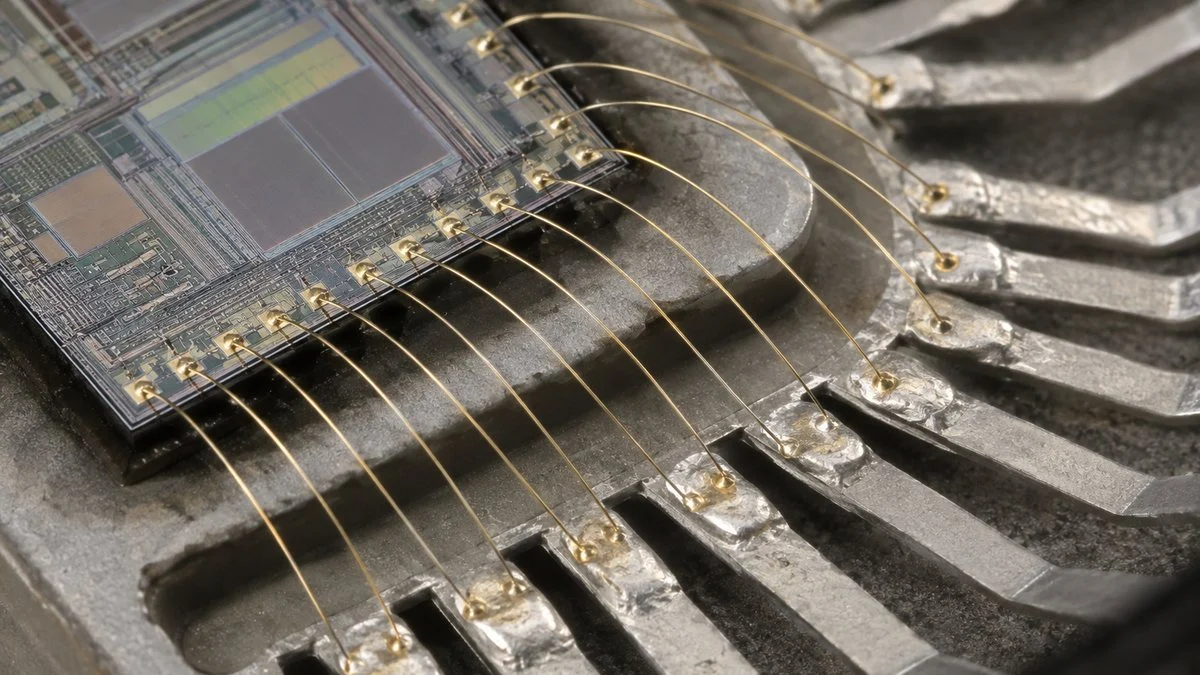
The flow below uses a lead-frame package, the type made in the largest numbers, as the example. The order and the steps used change with the product and package type, but the basic structure is the same.
It starts with testing at the wafer level, moves through assembly, and ends with final test.
Wafer test is sometimes counted as the last step of the front end. Some products also go through burn-in (high temperature and voltage) to remove early failures.
Back Grinding and Dicing
A wafer leaves the front end thick enough to survive processing without cracking. Back grinding uses a grinding wheel on the circuit-free back side to bring the wafer down to the thickness the package needs. This step matters most for thin smartphone packages and for memory, where several chips are stacked.
The thinned wafer is mounted on tape stretched across a ring frame and then goes to dicing. Most lines cut with a thin blade made of bonded diamond grit spinning at high speed; laser dicing is also used. Because the wafer stays on the tape, the chips do not scatter after cutting and can move to the next step together.
Die Bonding and Wire Bonding
Die bonding picks each cut chip (die) off the tape and fixes it to a set position on a lead frame or substrate with adhesive or solder. Misplacement or a poor bond here can lead to poor heat dissipation and broken connections later.
Wire bonding connects the aluminum pads around the edge of the chip (bonding pads) to the lead-frame terminals, one fine gold or aluminum wire at a time. The bonder strings wire at high speed, much like a sewing machine. For decades, it has been the standard way to connect a chip.
Molding and Finishing
Molding covers the connected chip and wires with an encapsulant such as epoxy resin. Lead frames are set in a mold, and heated, melted resin is injected to seal many chips at once. This is the step that gives a chip its familiar black body.
The exposed leads then get plating or another surface treatment so they solder well. Each part is cut from the lead frame, the leads are formed to shape, and a laser marks the maker's name, part number, and lot code.
Wafer Test and Final Test
Testing happens twice: once at the wafer level and once after packaging. In wafer test, a prober holds the wafer while the fine needles of a probe card touch each chip's electrodes, and a tester measures the electrical characteristics. Finding bad chips early means no packaging cost is wasted on them.
In final test, a handler inserts each packaged part into a socket, and the tester checks function and characteristics across temperatures. Some products also go through burn-in, which holds parts at high temperature and voltage to screen out those that would fail soon after they enter service. Camera-based inspection systems check for bent leads and faded markings, and AI visual inspection is being adopted for this job.
Where Japanese Suppliers Sit in the Back End
Japan's position in chips themselves has shrunk. Japan's Ministry of Economy, Trade and Industry (METI) put Japanese companies at 10.0% of world semiconductor sales in 2019, down from 50.3% in 1988. The equipment and materials picture is very different, and the back end is one of the clearest examples. The table maps back-end steps to the Japanese suppliers you are most likely to meet, with the share figure each company (or METI) has published.
| Back-end step | What is supplied | Japanese suppliers | Published share (basis, date) |
|---|---|---|---|
| Wafer test | Probers | Tokyo Electron, Tokyo Seimitsu (Accretech) | No company share figure found |
| Back grinding, dicing | Grinders, polishers, dicing saws | DISCO | 70–80% for both dicing saws and grinders/polishers (DISCO IR FAQ, "currently," no year) |
| Die bonding | Die bonding film (adhesive film that attaches and stacks chips) | Resonac | World No. 1 sales volume in 2024 (Resonac, citing Fuji Keizai) |
| Molding | Encapsulants (molding compounds) | Japanese makers as a group | About 80% held by Japanese companies (METI, March 2021, based on Nomura Securities data) |
| Molding | Molding equipment, including compression molding | TOWA | No verified figure found |
| Package substrate | ABF build-up film (insulating film between substrate layers) | Ajinomoto | Above 95% since launch (Ajinomoto briefing, June 2026) |
| Package substrate | Carrier-attached ultra-thin copper foil for fine circuits | Mitsui Kinzoku | 95% or more (product page, no year) |
| Package substrate | Substrates for high-end packages | Ibiden, Shinko Electric Industries | No company share figure found |
| Final test | Automated test equipment (ATE) | Advantest | 58% of the tester market in CY2024; 63% in memory testers, 56% in SoC testers (Advantest Investors' Guide, Oct. 2025) |
Read these figures with care. Each company defines its own market, some by units and some by revenue, and several give no year. Ajinomoto's share applies to one film inside the substrate, not to substrates as a whole. Do not compare the numbers with each other, and check the latest company report before using any of them in a sourcing decision.
The pattern is clear, though. Japanese companies are strongest in the tools and materials that touch the chip at every step: the saws and grinders that thin and cut it, the film that bonds it, the resin that seals it, the film inside its substrate, and the tester that clears it for shipment. For the wider list of Japanese top-share products, with sources, see Where Japan Holds Top Global Share: Materials and Equipment. The same pattern appears in passive components; see MLCC Manufacturing Process: Why Japanese Makers Lead.
Main Semiconductor Package Types
Packages differ in where the terminals come out and how much of the packaging work is done while the chips are still on the wafer. The right type depends on the application and the number of terminals needed.
The key differences are how the terminals come out and at what stage the chip is sealed.
BGA = ball grid array. WLCSP = wafer-level chip-scale package. FOWLP = fan-out wafer-level package. WLP (wafer-level packaging) is the general term for doing packaging steps on the whole wafer.
Lead-frame packages are simple and cheap, and they are still made in the largest numbers. When a processor needs hundreds or thousands of terminals, the sides of the package are not enough, so the BGA, with terminals across its whole bottom surface, became the main choice for high pin-count parts.
WLCSP and FOWLP do most of the packaging work at the wafer level. The finished part is close to the size of the chip, which suits devices that need small, thin components. FOWLP places cut chips back onto a carrier with gaps between them, fixes them in resin, and then routes wiring outward, so it can fit more terminals than the chip area alone would allow.
How Chips Connect: Wire Bonding, Flip Chip, and Hybrid Bonding
How the chip's electrodes connect to the outside matters as much as the package type. Wire bonding can only use pads around the edge of the chip, and each wire adds length to the electrical path.
Flip chip turns the chip face down and connects it directly to the substrate through small metal bumps formed on its electrodes. Electrodes can cover the whole chip surface and the paths are short, so many signals can pass through a small area with low resistance.
Hybrid bonding goes further by joining copper electrodes directly to each other. The much finer connection pitch it allows is a big part of what makes advanced packages perform.
The tighter the pitch, the more signal lines fit in the same area (shorter bar = higher density).
Typical values from a Tokyo Electron explainer. One hybrid bonding example reached 0.4 µm. Actual pitch varies by product and technology generation.
Hybrid bonding polishes chip surfaces extremely flat and bonds them together, insulating film and copper electrodes at the same time. With no bumps or solder, resistance and capacitance drop, so signals pass more easily with less delay. Sony introduced it in image sensors in 2016, and it has since spread to 3D NAND flash memory and other products.
What Is Advanced Packaging?
Advanced packaging is the general term for placing several chips side by side or stacking them inside one package so that they work like one large chip. A conventional package mainly protects a single chip. An advanced package connects chips densely enough to raise performance itself.
A typical example is the AI GPU (graphics processing unit), a processor built for graphics and parallel computing. Several stacks of high-bandwidth memory (HBM) sit next to the compute chip, and all of them connect through an interposer, an intermediate layer with very fine wiring. TSMC's CoWoS is a leading technology for this structure.
From top to bottom: chips, an intermediate wiring layer, and substrates.
Stacking chips vertically is called 3D packaging. More products now combine 2.5D and 3D.
Chiplets
Chiplets split circuits that used to sit on one large chip into smaller chips by function, such as compute, input/output (I/O), and memory, and then reassemble them in one package. Each function can use the process that suits it: the expensive leading-edge process can be reserved for the compute part, which needs the finest features, while I/O and other parts use proven processes.
Smaller chips also tend to improve yield, the share of good chips per wafer. On a large chip, a single defect on the wafer can scrap the whole die.
2.5D Packaging and Interposers
2.5D packaging places chips side by side on an interposer. The interposer carries wiring too fine for the package substrate, which lets the chips exchange large amounts of data at high speed.
Interposers have mostly been silicon, but they grow larger as more chips go on top. Developers are therefore working on interposers made of organic materials and produced on square panels instead of round wafers. Cutting square parts from a round wafer wastes the edge; a panel reduces that waste.
3D Stacking and HBM
3D packaging stacks chips vertically. HBM is the main example: many layers of DRAM dies, connected top to bottom by tiny vertical electrodes called through-silicon vias (TSVs).
In the 12-layer HBM3 that SK hynix announced in 2023, each DRAM die was made 40% thinner so that 12 layers fit in the same height as the earlier 8-layer product. This is where back grinding pays off. Thinning dies, keeping warpage and cracking under control, and stacking them accurately all depend on back-end precision and materials, and these directly decide the capacity and reliability of the product. SK hynix also uses a process called MR-MUF, which bonds the stacked dies in one step and fills the gaps between them with resin all at once.
Hybrid Bonding in Stacking
Bumps add height to every layer of a stack and limit how tight the pitch can get. Hybrid bonding eases both limits, so its use is expected to grow in memory stacking and in 3D connections between logic chips. Because it needs planarization and cleaning techniques close to those of the front end, it is also a clear sign that the line between front end and back end is blurring.
Why Advanced Packaging Matters Now
For decades, chip performance improved mainly by shrinking circuits. As shrinking became harder and more expensive, attention turned to the back end. Four factors explain why.
Making one chip bigger or finer is no longer enough to meet AI performance needs.
26 mm × 33 mm is the maximum exposure field listed in the specifications of an ASML lithography system.
1. Chip size has a physical ceiling. A lithography tool can print a circuit over an area of at most 26 mm × 33 mm (about 858 mm²) in one exposure, called the reticle field. A circuit larger than that cannot be made as one chip. For the largest processors, this ceiling blocks further gains, and the only way to add more circuitry is to connect several chips inside the package.
2. Yield and cost. As covered under chiplets, smaller dies and process mixing lower cost.
3. Distance to memory. In AI training and inference, the speed of moving data to and from memory often limits performance more than the computation itself. That is why the layout with HBM beside the compute chip is so widely used.
4. Market growth. Market research firm Yole Group put the advanced packaging market at $46 billion in 2024, up 19% from the year before, and forecasts it to exceed $79.4 billion by 2030. Mobile and consumer devices were the largest segment, at about 70% of 2024 revenue. The fastest-growing segment is telecom and infrastructure, which includes AI accelerators and GPUs, at a forecast 14.9% a year from 2024 to 2030.
At its April 2026 technology symposium, TSMC said it is already producing CoWoS packages 5.5 times the reticle size. It also plans to produce a 14-reticle CoWoS in 2028 that can hold about 10 large compute chips and 20 HBM stacks. Back-end capacity now helps decide how many AI chips can reach the market.
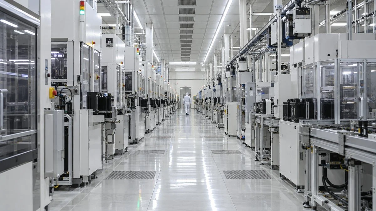
Who Does Back-End Work: OSATs, Foundries, and Japan
The chip industry divides design, front-end manufacturing, and back-end manufacturing among different companies. The back end includes chipmakers that do it in-house, contractors that specialize in it, and the equipment and materials suppliers behind both.
Companies that do assembly and test, and the equipment and materials companies that support them.
OSAT = outsourced semiconductor assembly and test. IDM = integrated device manufacturer. OSAT examples are taken from the 2022 revenue leaders shown in a Tokyo Electron explainer.
The top OSATs are Taiwanese, American, and Chinese. A Tokyo Electron explainer sums up Japan's position this way: strong in back-end equipment and materials, but not clearly strong in the contract assembly-and-test business itself. For a buyer, this means you will often deal with a non-Japanese OSAT while the tools and materials on its line come from Japan.
Related: Top Japanese Semiconductor and Electronic Component Makers
Advanced Packaging Projects in Japan
Advanced packaging has drawn a wave of R&D and pilot-line projects to Japan. A common thread is partnering with Japanese equipment and materials makers to develop the technology.
Work is moving in three directions: R&D, prototyping, and automation.
Years show the center opening, association founding, planned R&D start, or planned prototype-line start. Based on each organization's announcements. RDL = redistribution layer. AIST = National Institute of Advanced Industrial Science and Technology.
R&D Centers: TSMC and Rapidus
TSMC set up an R&D subsidiary in Japan in 2021 and completed a clean room at AIST's Tsukuba Center in 2022. Its development work with Japanese partners covers:
- Materials such as thermal interface materials, encapsulants, underfill, and solder
- Package substrates
- Equipment
- Metrology and inspection
Rapidus aims to mass-produce leading-edge 2 nm logic chips. It has also set up a back-end R&D center, Rapidus Chiplet Solutions, inside a Seiko Epson site in Chitose, Hokkaido. Its 2024 announcement planned equipment move-in from April 2025 and the start of R&D in April 2026, with the goal of developing front-end and back-end processes together at nearby sites.
Materials Consortium and Automation: JOINT3 and SATAS
In September 2025, Resonac launched JOINT3, a consortium of 27 companies from Japan and overseas. Under the plan, a line at a Resonac site in Yuki, Ibaraki, prototypes organic interposers on 515 × 510 mm (about 20 × 20 in) panels, with operation scheduled for 2026, and member companies jointly evaluate materials, equipment, and design tools.
SATAS takes on the labor-intensive side of the back end. It is a technology research association founded in April 2024 by Intel, Omron, and other companies to reduce labor in and automate assembly and test, and to develop the industry standards needed to do so.
Questions to Ask a Japanese Back-End Supplier
Japanese equipment and materials makers often send field engineers to a customer's plant to bring up a new process together. Back-end problems often surface one step later. A misplaced or poorly bonded die, for example, can cause poor heat dissipation or broken connections further down the line. Raise these questions before evaluation starts.
On the Japanese side, several roles may join the discussion. Production and process engineers bring up the process and tune conditions; their typical challenges are grinding thin dies without cracking them, placing dies without misalignment, and filling resin without voids. Quality assurance traces what went wrong, and at which step, using wafer test and final test results and failure analysis. Technical sales staff from equipment and materials makers work alongside their field engineers. In advanced packaging, materials and heat must be considered from the design stage, so bring these people in early. For background on these roles, see Seisan Gijutsu: Japanese Production Engineering Explained and QA vs QC in Japanese Companies.
Checklist Before Qualifying a Tool or Material
- Process window: the wafer thickness, die size, and die stack height the tool or material has been qualified for
- Upstream and downstream fit: which tapes, adhesives, encapsulants, or substrates it has been tested with, and which combinations are not recommended
- Reference data: reliability results (for example, moisture sensitivity or temperature cycling) and the test conditions behind them
- Local support: whether field engineers and spare parts are based in your country or region, and the response time
- Supply continuity: lead time, minimum order, which plant makes the product, and whether a second plant can supply it
- Change notification: how and how far in advance you will be told about changes in formulation, plant, or key raw materials
- Documentation language: whether manuals, safety data sheets, and certificates of analysis are available in English
- Share claims: if the supplier quotes a market share, the market definition, year, and source behind it
Sample Inquiry Email
Adjust the bracketed parts and send it to the supplier's overseas sales office or local distributor.
Subject: Technical inquiry – [product name] for [package type] assembly

Dear [Name],

We are evaluating [product name] for our [package type] line at our
[city, country] assembly and test site. Could you share the following?

1. Qualified range: wafer thickness, die size, and stack height
2. Materials and tools it has been tested with in the steps before
   and after, and any combinations you do not recommend
3. Reliability data and the test conditions used
4. Lead time, minimum order quantity, and producing plant(s)
5. Your change-notification process (formulation, plant, raw materials)
6. Local field support and spare parts coverage in [country]
7. English versions of the manual, SDS, and certificate of analysis

We plan to start evaluation in [month/year]. Thank you for your support.

Best regards,
[Your name, title, company]
Limits of This Guide
- The process flow is a general one based on a lead-frame package. Steps, order, and equipment differ by product, package type, and company.
- Share figures are published by the companies themselves or by METI. We did not check them against independent market data, several give no year, and the METI figure for encapsulants is from a 2021 document.
- The supplier table lists the Japanese companies most often named at each step. It is not a complete list, and non-Japanese suppliers also compete at every step.
- Projects in Japan are described from announcements. Schedules may have changed since.
FAQ
What is the back-end process in semiconductor manufacturing?
It is the part of chipmaking that turns a finished wafer into packaged, tested chips. The usual steps are wafer test, back grinding, dicing, die bonding, wire bonding (or flip-chip bonding), molding, finishing, and final test.
What is the difference between front-end and back-end semiconductor processes?
The front end builds circuits on the wafer with nanometer-scale processing and is capital-intensive. The back end cuts the wafer into chips, packages them, and tests them, and has traditionally been more labor-intensive. Advanced packaging, especially hybrid bonding, is blurring the line between the two.
Which Japanese companies make semiconductor back-end equipment?
Examples include DISCO (dicing saws and grinders), Advantest (test systems), Tokyo Electron and Tokyo Seimitsu (probers), and TOWA (molding equipment). DISCO publishes a 70–80% share for dicing saws and grinders, and Advantest a 58% tester share for CY2024.
Why does advanced packaging matter for AI chips?
The largest AI processors need more circuitry than one die can hold, and AI workloads need very fast access to memory. Advanced packaging connects several compute chips and HBM stacks on an interposer so they act like one large chip. TSMC is already producing CoWoS packages 5.5 times the reticle size.
What is ABF and who makes it?
ABF (Ajinomoto Build-up Film) is the insulating film between the wiring layers of high-end package substrates. Ajinomoto, better known as a food company, makes it and says ABF has held a share above 95% since launch.
Sources
- Back-end process steps: JFE Shoji Electronics, "What Is the Semiconductor Back-End Process?" (Japanese); Yoshida SKT, "What Is the Semiconductor Back-End Process?" (Japanese)
- Package types and flip chip: IR Engineer Education Institute, "Basics of Semiconductor Packaging" (Japanese)
- Wafer test and final test: Advantest, "What Is ATE?" (Japanese)
- Connection pitch and hybrid bonding: Tokyo Electron, TELESCOPE Magazine, hybrid bonding (Japanese)
- OSATs and Japan's position: Tokyo Electron, TELESCOPE Magazine, the position of OSATs (Japanese)
- 12-layer HBM3: SK hynix Newsroom, "SK hynix Develops Industry's First 12-Layer HBM3," April 20, 2023
- Exposure field size: ASML, TWINSCAN NXT:1980Di
- CoWoS size: TSMC, "TSMC Debuts A13 Technology at 2026 North America Technology Symposium," April 23, 2026
- Advanced packaging market: Yole Group, "Advanced Packaging Market Set to Reach $79.4 Billion by 2030," via Edge AI and Vision Alliance, September 2025
- Japan's chip sales share and encapsulant share: METI, Semiconductor Strategy outline, March 2021 (Japanese)
- DISCO: IR FAQ (Japanese)
- Advantest: Investors' Guide, October 2025 (Japanese)
- Resonac die bonding film: Resonac Now, September 1, 2025 (Japanese)
- Ajinomoto: Electronic materials business briefing, June 30, 2026 (Japanese)
- Mitsui Kinzoku: MicroThin carrier-attached ultra-thin copper foil (Japanese)
- TSMC Japan 3DIC R&D Center: TSMC, About the TSMC Japan 3DIC R&D Center (Japanese)
- Rapidus Chiplet Solutions: Rapidus, back-end R&D center announcement, October 3, 2024
- JOINT3: Resonac, JOINT3 consortium of 27 companies, September 3, 2025 (Japanese)
- SATAS: SATAS, organization overview (Japanese); EE Times Japan, SATAS founded by Intel, Omron, and others (Japanese)
Original article in JapaneseThis guide is adapted from a MONOSCOPE article written for readers in Japan: 半導体の後工程とは?工程の流れと先端パッケージが注目される理由
About the editor
 MONOSCOPE EditorFOUNDER & EDITOR
Spent about ten years at a plant equipment maker and a plant engineering company, proposing, designing, and commissioning equipment, then moved into web marketing. Now a web consultant for B2B manufacturers, helping them explain their products and technology. Licensed in Japan as an Energy Manager and a Third-Class Chief Electrical Engineer.
Has run an engineering blog since 2017 (500+ articles) and a Japanese YouTube channel with about 20,000 subscribers. Each English guide is written from the Japanese shop-floor point of view and checked against the cited standards.